- 您現(xiàn)在的位置:買(mǎi)賣(mài)IC網(wǎng) > PDF目錄223633 > CX77304-17 (SKYWORKS SOLUTIONS INC) YTQ-125-01-L-Q 2MM STACK OCTOPUS AUG 22/02 HI DENSITY STACKER PDF資料下載
參數(shù)資料
| 型號(hào): | CX77304-17 |
| 廠(chǎng)商: | SKYWORKS SOLUTIONS INC |
| 元件分類(lèi): | 放大器 |
| 英文描述: | YTQ-125-01-L-Q 2MM STACK OCTOPUS AUG 22/02 HI DENSITY STACKER |
| 中文描述: | 880 MHz - 915 MHz RF/MICROWAVE NARROW BAND MEDIUM POWER AMPLIFIER |
| 封裝: | 9.10 X 11.60 MM, 1.50 MM HEIGHT, LEAD FREE, LEADLESS, PLASTIC, SO-16 |
| 文件頁(yè)數(shù): | 4/15頁(yè) |
| 文件大小: | 605K |
| 代理商: | CX77304-17 |
第1頁(yè)第2頁(yè)第3頁(yè)當(dāng)前第4頁(yè)第5頁(yè)第6頁(yè)第7頁(yè)第8頁(yè)第9頁(yè)第10頁(yè)第11頁(yè)第12頁(yè)第13頁(yè)第14頁(yè)第15頁(yè)
DATA SHEET CX77304-17
PA MODULE FOR TRI-BAND EGSM DCS PCS / GPRS
Skyworks Solutions, Inc. Phone [781] 376-3000 Fax [781] 376-3100 sales@skyworksinc.com www.skyworksinc.com
12
July 29, 2004 Skyworks Proprietary and Confidential Information Products and Product Information are Subject to Change Without Notice. 101943B
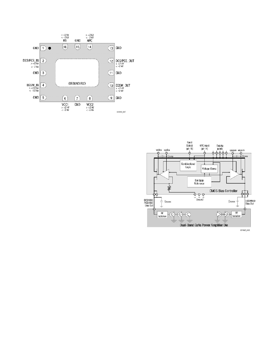
Figure 7. ESD Sensitivity Areas
Various failure criteria can be utilized when performing ESD
testing. Many vendors employ relaxed ESD failure standards,
which fail devices only after “the pin fails the electrical
specification limits” or “the pin becomes completely non-
functional”. Skyworks employs most stringent criteria, fails
devices as soon as the pin begins to show any degradation on a
curve tracer.
To avoid ESD damage, latent or visible, it is very important the
Class-1 ESD handling precautions listed below are observed in
the product assembly and test areas.
Personnel Grounding
-
Wrist Straps
-
Conductive Smocks, Gloves and Finger Cots
-
Antistatic ID Badges
Facility
-
Relative Humidity Control and Air Ionizers
-
Dissipative Floors (less than 109
to GND)
Protective Workstation
-
Dissipative Table Tops
-
Protective Test Equipment (Properly Grounded)
-
Grounded Tip Soldering Irons
-
Conductive Solder Suckers
-
Static Sensors
Protective Packaging & Transportation
-
Bags and Pouches (Faraday Shield)
-
Protective Tote Boxes (Conductive Static Shielding)
-
Protective Trays
-
Grounded Carts
-
Protective Work Order Holders
Technical Information
CMOS Bias Controller Characteristics
The CMOS die within the PAM performs several functions that are
important to the overall module performance. Some of these
functions must be considered for development of the power
ramping features in a 3GPP compliant transmitter power control
loop. Power ramping considerations will be discussed later in this
section.
NOTE:
Please refer to 3GPP TS 05.05, Digital Cellular
Communications System (Phase 2+); Radio Transmission
and Reception. All GSM specifications are now the
responsibility of 3GPP. The standards are available at
http://www.3GPP.org/specs/specs.htm
The four main functions described in this section are Standby
Mode Control, Band Select, Voltage Clamp, and Current Buffer.
The functional block diagram is shown in Figure 8.
Figure 8. Functional Block Diagram
Standby Mode Control
The Combinational Logic cell includes enable circuitry that
monitors the APC ramping voltage from the power amplifier
controller (PAC) circuit in the GSM transmitter. Typical handset
designs directly connect the PA VCC to the battery at all times, and
for some PA manufacturers this requires a control signal to set
the device in or out of standby mode. The Skyworks PAM does
not require a Transmit Enable input because it contains a standby
detection circuit that senses the VAPC to enable or disable the PA.
This feature helps minimize battery discharge when the PA is in
standby mode. When VAPC is below the enable threshold voltage,
the PA goes into a standby mode, which reduces battery current
(ICC) to 6
A, typical, under nominal conditions.
相關(guān)PDF資料 |
PDF描述 |
|---|---|
| CX805-30 | CX805-30 Baseband Processor for Multiband GSM and GPRS Applications |
| CXA10-48D05 | 2-OUTPUT 10 W DC-DC REG PWR SUPPLY MODULE |
| CXA1786N-T4 | PHASE LOCKED LOOP, 1100 MHz, PDSO20 |
| CXD5-15 | 2-OUTPUT DC-DC REG PWR SUPPLY MODULE |
| CXK79M36C160GB-33 | 512K X 36 STANDARD SRAM, 1.8 ns, PBGA209 |
相關(guān)代理商/技術(shù)參數(shù) |
參數(shù)描述 |
|---|---|
| CX77306-11P | 制造商:Cypress Semiconductor 功能描述:CX77306-11P 制造商:Skyworks Solutions Inc 功能描述:CX77306-11P |
| CX77312 | 制造商:未知廠(chǎng)家 制造商全稱(chēng):未知廠(chǎng)家 功能描述:CX77312 Product Summary|PA Modules for GSM/GPRS Handsets |
| CX77314 | 制造商:未知廠(chǎng)家 制造商全稱(chēng):未知廠(chǎng)家 功能描述:CX77314 Product Summary|PA Modules for GSM/GPRS Handsets |
| CX77315 | 制造商:未知廠(chǎng)家 制造商全稱(chēng):未知廠(chǎng)家 功能描述:CX77315 Product Summary|PA Modules for GSM/GPRS Handsets |
| CX7792-000 | 制造商:TE Connectivity 功能描述:WXA-0202-0-9CS3264 - Bulk |
發(fā)布緊急采購(gòu),3分鐘左右您將得到回復(fù)。