- 您現(xiàn)在的位置:買賣IC網(wǎng) > PDF目錄379830 > CDC2509PW (Texas Instruments, Inc.) 3.3-V PHASE-LOCK LOOP CLOCK DRIVER PDF資料下載
參數(shù)資料
| 型號: | CDC2509PW |
| 廠商: | Texas Instruments, Inc. |
| 英文描述: | 3.3-V PHASE-LOCK LOOP CLOCK DRIVER |
| 中文描述: | 3.3 - V相位鎖相環(huán)時鐘驅(qū)動器 |
| 文件頁數(shù): | 1/9頁 |
| 文件大小: | 132K |
| 代理商: | CDC2509PW |
CDC2509
3.3-V PHASE-LOCK LOOP CLOCK DRIVER
SCAS580A – OCTOBER 1996 – REVISED JANUARY 1998
1
POST OFFICE BOX 655303
DALLAS, TEXAS 75265
Phase-Lock Loop Clock Distribution for
Synchronous DRAM Applications
Distributes One Clock Input to One Bank of
Five and One Bank of Four Outputs
Separate Output Enable for Each Output
Bank
External Feedback (FBIN) Pin Is Used to
Synchronize the Outputs to the Clock Input
On-Chip Series Damping Resistors
No External RC Network Required
Operates at 3.3-V V
CC
Packaged in Plastic 24-Pin Thin Shrink
Small-Outline Package
description
The CDC2509 is a high-performance, low-skew, low-jitter, phase-lock loop (PLL) clock driver. It uses a PLL to
precisely align, in both frequency and phase, the feedback (FBOUT) output to the clock (CLK) input signal. It
is specifically designed for use with synchronous DRAMs. The CDC2509 operates at 3.3-V V
CC
and provides
integrated series-damping resistors that make it ideal for driving point-to-point loads.
One bank of five outputs and one bank of four outputs provide nine low-skew, low-jitter copies of CLK. Output
signal duty cycles are adjusted to 50 percent, independent of the duty cycle at CLK. Each bank of outputs can
be enabled or disabled separately via the control (1G and 2G) inputs. When the G inputs are high, the outputs
switch in phase and frequency with CLK; when the G inputs are low, the outputs are disabled to the logic-low
state.
Unlike many products containing PLLs, the CDC2509 does not require external RC networks. The loop filter
for the PLL is included on-chip, minimizing component count, board space, and cost.
Because it is based on PLL circuitry, the CDC2509 requires a stabilization time to achieve phase lock of the
feedback signal to the reference signal. This stabilization time is required, following power up and application
of a fixed-frequency, fixed-phase signal at CLK, as well as following any changes to the PLL reference or
feedback signals. The PLL can be bypassed for test purposes by strapping AV
CC
to ground.
The CDC2509 is characterized for operation from 0
°
C to 70
°
C.
FUNCTION TABLE
INPUTS
OUTPUTS
1G
2G
CLK
1Y
(0:4)
2Y
(0:3)
FBOUT
X
X
L
L
L
L
L
L
H
L
L
H
L
H
H
L
H
H
H
L
H
H
L
H
H
H
H
H
H
H
Copyright
1998, Texas Instruments Incorporated
PRODUCTION DATA information is current as of publication date.
Products conform to specifications per the terms of Texas Instruments
standard warranty. Production processing does not necessarily include
testing of all parameters.
Please be aware that an important notice concerning availability, standard warranty, and use in critical applications of
Texas Instruments semiconductor products and disclaimers thereto appears at the end of this data sheet.
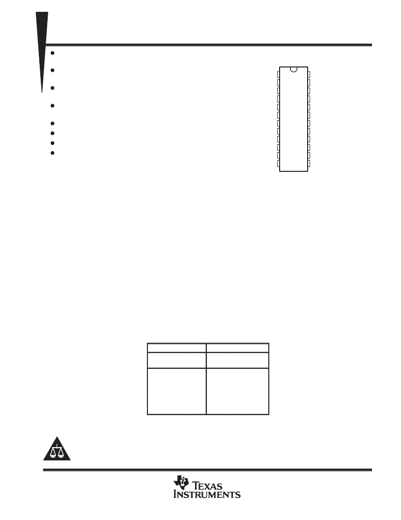
CLK
AV
CC
V
CC
2Y0
2Y1
GND
GND
2Y2
2Y3
V
CC
2G
FBIN
1
2
3
4
5
6
7
8
9
10
11
12
AGND
V
CC
1Y0
1Y1
1Y2
GND
GND
1Y3
1Y4
V
CC
1G
FBOUT
24
23
22
21
20
19
18
17
16
15
14
13
PW PACKAGE
(TOP VIEW)
相關(guān)PDF資料 |
PDF描述 |
|---|---|
| CDC2510APWRG4 | 3.3-V PHASE-LOCK LOOP CLOCK DRIVER |
| CDC2510BPW | 3.3-V PHASE-LOCK LOOP CLOCK DRIVER |
| CDC2510PW | 3.3-V PHASE-LOCK LOOP CLOCK DRIVER |
| CDC2516DGG | 3.3-V PHASE-LOCK LOOP CLOCK DRIVER |
| CDC2587 | Octal Divided -by-2 Circuit/Clock Driver(3.3V鎖相環(huán)時鐘驅(qū)動器(三態(tài)輸出)) |
相關(guān)代理商/技術(shù)參數(shù) |
參數(shù)描述 |
|---|---|
| CDC2509PWLE | 制造商:未知廠家 制造商全稱:未知廠家 功能描述:Nine Distributed-Output Clock Driver |
| CDC2509PWR | 功能描述:時鐘驅(qū)動器及分配 3.3V Ph-Lock Loop Clock Driver RoHS:否 制造商:Micrel 乘法/除法因子:1:4 輸出類型:Differential 最大輸出頻率:4.2 GHz 電源電壓-最大: 電源電壓-最小:5 V 最大工作溫度:+ 85 C 封裝 / 箱體:SOIC-8 封裝:Reel |
| CDC2509PWRG4 | 功能描述:時鐘驅(qū)動器及分配 3.3V Ph-Lock Loop Clock Driver RoHS:否 制造商:Micrel 乘法/除法因子:1:4 輸出類型:Differential 最大輸出頻率:4.2 GHz 電源電壓-最大: 電源電壓-最小:5 V 最大工作溫度:+ 85 C 封裝 / 箱體:SOIC-8 封裝:Reel |
| CDC2510 | 制造商:TI 制造商全稱:Texas Instruments 功能描述:3.3-V PHASE-LOCK LOOP CLOCK DRIVER |
| CDC2510A | 制造商:未知廠家 制造商全稱:未知廠家 功能描述:3.3-V Phase-Lock Loop Clock Driver |
發(fā)布緊急采購,3分鐘左右您將得到回復。