- 您現(xiàn)在的位置:買賣IC網(wǎng) > PDF目錄295217 > CBTD3257PW (NXP SEMICONDUCTORS) QUAD 2-CHANNEL, SGL ENDED MULTIPLEXER, PDSO16 PDF資料下載
參數(shù)資料
| 型號(hào): | CBTD3257PW |
| 廠商: | NXP SEMICONDUCTORS |
| 元件分類: | 多路復(fù)用及模擬開關(guān) |
| 英文描述: | QUAD 2-CHANNEL, SGL ENDED MULTIPLEXER, PDSO16 |
| 封裝: | 4.40 MM, PLASTIC, MO-153, SOT403-1, TSSOP-16 |
| 文件頁數(shù): | 6/11頁 |
| 文件大?。?/td> | 94K |
| 代理商: | CBTD3257PW |
Philips Semiconductors
Preliminary data
CBTD3257
Quad 1-of-2 multiplexer/demultiplexer
with level shifting
2002 Sep 09
4
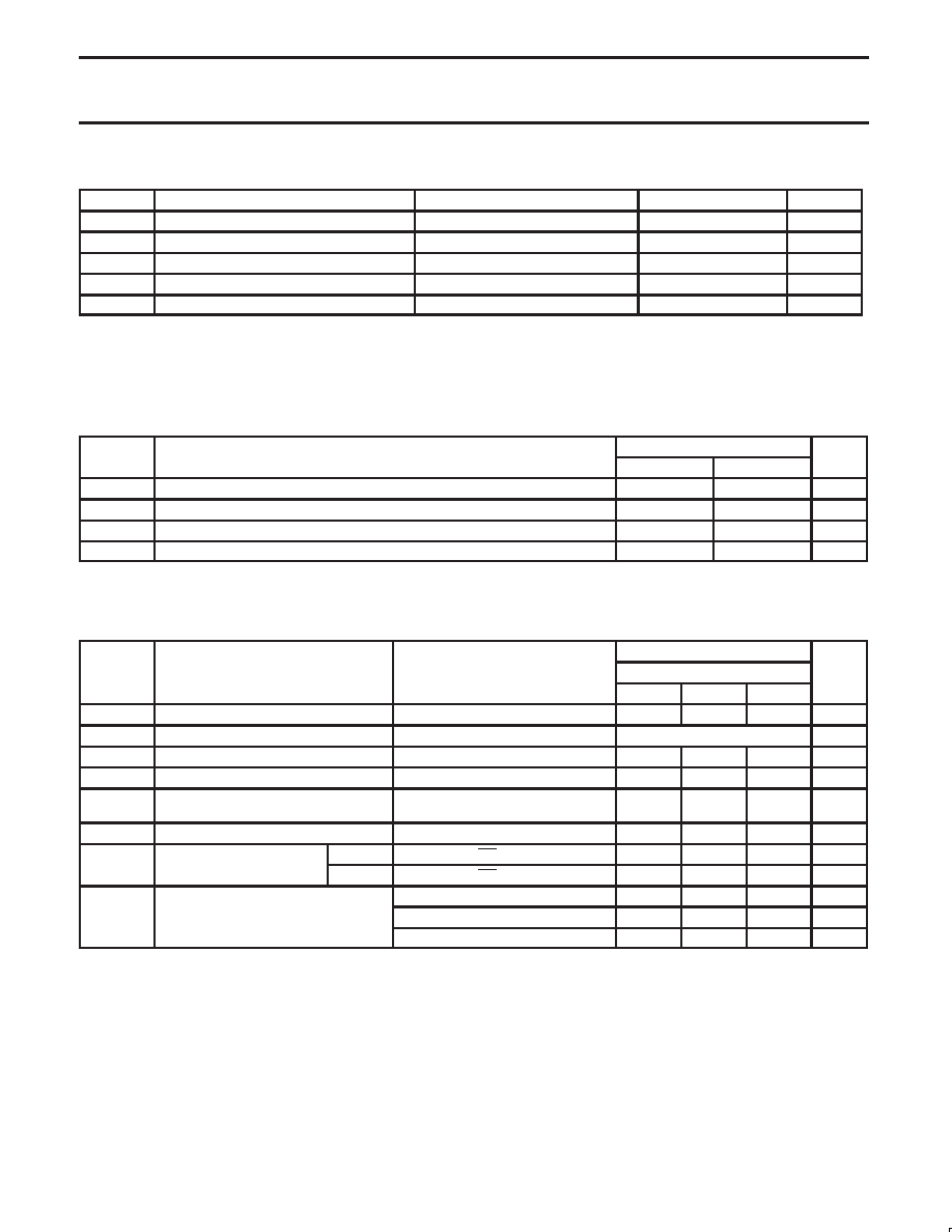
ABSOLUTE MAXIMUM RATINGS1
SYMBOL
PARAMETER
CONDITIONS
RATING
UNIT
VCC
DC supply voltage
–0.5 to +7.0
V
VI
DC input voltage2
–0.5 to +7.0
V
Continuous channel current
128
mA
IK
Input clamp current
VI/O < 0
–50
mA
Tstg
Storage temperature range
–65 to +150
°C
NOTES:
1. Stresses beyond those listed may cause permanent damage to the device. These are stress ratings only and functional operation of the
device at these or any other conditions beyond those indicated under “recommended operating conditions” is not implied. Exposure to
absolute-maximum-rated conditions for extended periods may affect device reliability.
2. The input and output negative-voltage ratings may be exceeded if the input and output clamp-current ratings are observed.
RECOMMENDED OPERATING CONDITIONS
SYMBOL
PARAMETER
LIMITS
UNIT
SYMBOL
PARAMETER
MIN
MAX
UNIT
VCC
DC supply voltage
4.5
5.5
V
VIH
High-level input voltage
2.0
—
V
VIL
Low-level Input voltage
—
0.8
V
Tamb
Operating free-air temperature range
–40
+85
°C
NOTE:
1. All unused control inputs of the device must be held at VCC or GND to ensure proper device operation.
DC ELECTRICAL CHARACTERISTICS
LIMITS
SYMBOL
PARAMETER
TEST CONDITIONS
Tamb = –40 to +85 °C
UNIT
MIN
TYP1
MAX
VIK
Input clamp voltage
VCC = 4.5 V; II = –18 mA
—
–1.2
V
VP
Pass voltage
VI = VCC = 5.5 V; I/O = –100 mA
See Figure 1
II
Input leakage current
VCC = 5.5 V; VI = GND or 5.5 V
—
±1
A
ICC
Quiescent supply current
VCC = 5.5 V; IO = 0, VI = VCC or GND
—
1.5
mA
ICC
Additional supply current per input pin2
VCC = 5.5 V, one input at 3.4 V,
other inputs at VCC or GND
—
2.5
mA
CI
Control pins
VI= 3 V or 0
—
4.5
—
pF
C O(O )
Power off leakage current
A port
VO = 3 V or 0; OE = VCC
—
12.5
—
pF
CIO(OFF)
Power-off leakage current
B port
VO = 3 V or 0; OE = VCC
—
6.5
—
pF
3
VCC = 4.5 V; VI = 0V; II = 64 mA
—
5
7
ron3
On-resistance
VCC = 4.5 V; VI = 0V; II = 30 mA
—
5
7
VCC = 4.5 V; VI = 2.4 V; II = 15 mA
—
16
50
NOTES:
1. All typical values are at VCC = 5 V, Tamb = 25 °C.
2. This is the increase in supply current for each input that is at the specified TTL voltage level rather than VCC or GND
3. Measured by the voltage drop between the A and the B terminals at the indicated current through the switch.
On-state resistance is determined by the lowest voltage of the two (A or B) terminals.
相關(guān)PDF資料 |
PDF描述 |
|---|---|
| CC045-FREQTS-OUT27 | CRYSTAL OSCILLATOR, CLOCK, 2.5 MHz - 55 MHz, HCMOS OUTPUT |
| CC045Z-FREQTS-OUT27 | CRYSTAL OSCILLATOR, CLOCK, 2.5 MHz - 55 MHz, HCMOS OUTPUT |
| CC045EZ-FREQTS-OUT27 | CRYSTAL OSCILLATOR, CLOCK, 2.5 MHz - 55 MHz, HCMOS OUTPUT |
| CC045L-B245-FREQTS-OUT27 | CRYSTAL OSCILLATOR, CLOCK, 2.5 MHz - 55 MHz, HCMOS OUTPUT |
| CC045EZ-B2-FREQTS-OUT27 | CRYSTAL OSCILLATOR, CLOCK, 2.5 MHz - 55 MHz, HCMOS OUTPUT |
相關(guān)代理商/技術(shù)參數(shù) |
參數(shù)描述 |
|---|---|
| CBTD3306 | 制造商:PHILIPS 制造商全稱:NXP Semiconductors 功能描述:Dual bus switch with level shifting |
| CBTD3306_11 | 制造商:PHILIPS 制造商全稱:NXP Semiconductors 功能描述:Dual bus switch with level shifting Multiple package options |
| CBTD3306D | 功能描述:數(shù)字總線開關(guān) IC DUAL BUS SWITCH W/LEVEL SHIFT RoHS:否 制造商:Texas Instruments 開關(guān)數(shù)量:24 傳播延遲時(shí)間:0.25 ns 最大工作溫度:+ 85 C 最小工作溫度:- 40 C 封裝 / 箱體:TSSOP-56 封裝:Reel |
| CBTD3306D,112 | 功能描述:數(shù)字總線開關(guān) IC DUAL BUS SWITCH RoHS:否 制造商:Texas Instruments 開關(guān)數(shù)量:24 傳播延遲時(shí)間:0.25 ns 最大工作溫度:+ 85 C 最小工作溫度:- 40 C 封裝 / 箱體:TSSOP-56 封裝:Reel |
| CBTD3306D,118 | 功能描述:數(shù)字總線開關(guān) IC DUAL BUS SWITCH RoHS:否 制造商:Texas Instruments 開關(guān)數(shù)量:24 傳播延遲時(shí)間:0.25 ns 最大工作溫度:+ 85 C 最小工作溫度:- 40 C 封裝 / 箱體:TSSOP-56 封裝:Reel |
發(fā)布緊急采購,3分鐘左右您將得到回復(fù)。