- 您現(xiàn)在的位置:買賣IC網(wǎng) > PDF目錄211158 > CAT93C57V 128 X 16 MICROWIRE BUS SERIAL EEPROM, PDSO8 PDF資料下載
參數(shù)資料
| 型號(hào): | CAT93C57V |
| 元件分類: | PROM |
| 英文描述: | 128 X 16 MICROWIRE BUS SERIAL EEPROM, PDSO8 |
| 封裝: | LEAD AND HALOGEN FREE, SOIC-8 |
| 文件頁數(shù): | 8/10頁 |
| 文件大?。?/td> | 80K |
| 代理商: | CAT93C57V |
7
93C46/56/57/66/86
Doc. No. 1023, Rev. J
The format for all instructions sent to the device is a
logical "1" start bit, a 2-bit (or 4-bit) opcode, 6-bit (93C46)/
/7-bit (93C57)/ 8-bit (93C56 or 93C66)/10-bit (93C86)
(an additional bit when organized X8) and for write
operations a 16-bit data field (8-bit for X8 organizations).
Note: This note is applicable only to 93C86. The Write,
Erase, Write all and Erase all instructions require PE=1.
If PE is left floating, 93C86 is in Program Enabled mode.
For Write Enable and Write Disable instruction PE=don’t
care.
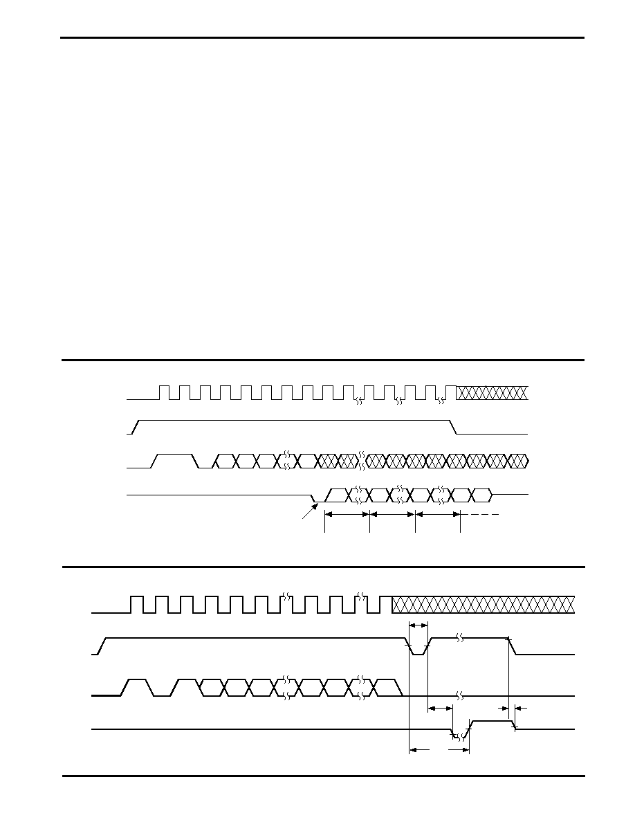
Read
Upon receiving a READ command and an address
(clocked into the DI pin), the DO pin of the CAT93C46/
56/57/66/86 will come out of the high impedance state
and, after sending an initial dummy zero bit, will begin
shifting out the data addressed (MSB first). The output
data bits will toggle on the rising edge of the SK clock and
are stable after the specified time delay (tPD0 or tPD1).
For the CAT93C56/57/66/86, after the initial data word
has been shifted out and CS remains asserted with the
SK clock continuing to toggle, the device will automatically
increment to the next address and shift out the next data
word in a sequential READ mode. As long as CS is
continuously asserted and SK continues to toggle, the
device will keep incrementing to the next address
automatically until it reaches to the end of the address
space, then loops back to address 0. In the sequential
READ mode, only the initial data word is preceeded by
a dummy zero bit. All subsequent data words will follow
without a dummy zero bit.
Write
After receiving a WRITE command, address and the
data, the CS (Chip Select) pin must be deselected for a
minimum of tCSMIN. The falling edge of CS will start the
self clocking clear and data store cycle of the memory
location specified in the instruction. The clocking of the
SK pin is not necessary after the device has entered the
self clocking mode. The ready/busy status of the
CAT93C46/56/57/66/86 can be determined by selecting
the device and polling the DO pin. Since this device
features Auto-Clear before write, it is NOT necessary to
erase a memory location before it is written into.
Figure 3. Write Instruction Timing
93C46/56/57/66/86 F05
Figure 2b. Read Instruction Timing (93C56/57/66/86)
SK
CS
DI
DO
HIGH-Z
11
0
AN AN–1
A0
Dummy 0
D15 . . . D0
or
D7 . . . D0
1
1111111
Address + 1
D15 . . . D0
or
D7 . . . D0
Address + 2
D15 . . . D0
or
D7 . . . D0
Address + n
D15 . . .
or
D7 . . .
Don't Care
SK
CS
DI
DO
tCSMIN
STANDBY
HIGH-Z
101
AN AN-1
A0
DN
D0
BUSY
READY
STATUS
VERIFY
tSV
tHZ
tEW
相關(guān)PDF資料 |
PDF描述 |
|---|---|
| CAT93C57YA-1.8TE13 | 128 X 16 MICROWIRE BUS SERIAL EEPROM, PDSO8 |
| CO-202G38HJAT10MHZ | OCXO, CLOCK, 10 MHz, TTL OUTPUT |
| CO-202G38JL1AT1MHZ | OCXO, CLOCK, 1 MHz, TTL OUTPUT |
| CO-202A19JL1AT5MHZ | OCXO, CLOCK, 5 MHz, TTL OUTPUT |
| CO-202A19KL1AT10MHZ | OCXO, CLOCK, 10 MHz, TTL OUTPUT |
相關(guān)代理商/技術(shù)參數(shù) |
參數(shù)描述 |
|---|---|
| CAT93C57V-1.8 | 功能描述:電可擦除可編程只讀存儲(chǔ)器 (256x8) (128x16) 2K RoHS:否 制造商:Atmel 存儲(chǔ)容量:2 Kbit 組織:256 B x 8 數(shù)據(jù)保留:100 yr 最大時(shí)鐘頻率:1000 KHz 最大工作電流:6 uA 工作電源電壓:1.7 V to 5.5 V 最大工作溫度:+ 85 C 安裝風(fēng)格:SMD/SMT 封裝 / 箱體:SOIC-8 |
| CAT93C57V-1.8TE13 | 制造商:未知廠家 制造商全稱:未知廠家 功能描述:EEPROM |
| CAT93C57V-25628 | 制造商:Catalyst Semiconductor 功能描述: |
| CAT93C57V-26528 | 制造商:Rochester Electronics LLC 功能描述: 制造商:Catalyst Semiconductor 功能描述: |
| CAT93C57V-26528T | 制造商:Rochester Electronics LLC 功能描述: 制造商:Catalyst Semiconductor 功能描述: |
發(fā)布緊急采購,3分鐘左右您將得到回復(fù)。