- 您現(xiàn)在的位置:買賣IC網(wǎng) > PDF目錄210366 > BX80532KC1900E (INTEL CORP) 1900 MHz, MICROPROCESSOR PDF資料下載
參數(shù)資料
| 型號: | BX80532KC1900E |
| 廠商: | INTEL CORP |
| 元件分類: | 微控制器/微處理器 |
| 英文描述: | 1900 MHz, MICROPROCESSOR |
| 文件頁數(shù): | 21/132頁 |
| 文件大小: | 2316K |
| 代理商: | BX80532KC1900E |
第1頁第2頁第3頁第4頁第5頁第6頁第7頁第8頁第9頁第10頁第11頁第12頁第13頁第14頁第15頁第16頁第17頁第18頁第19頁第20頁當(dāng)前第21頁第22頁第23頁第24頁第25頁第26頁第27頁第28頁第29頁第30頁第31頁第32頁第33頁第34頁第35頁第36頁第37頁第38頁第39頁第40頁第41頁第42頁第43頁第44頁第45頁第46頁第47頁第48頁第49頁第50頁第51頁第52頁第53頁第54頁第55頁第56頁第57頁第58頁第59頁第60頁第61頁第62頁第63頁第64頁第65頁第66頁第67頁第68頁第69頁第70頁第71頁第72頁第73頁第74頁第75頁第76頁第77頁第78頁第79頁第80頁第81頁第82頁第83頁第84頁第85頁第86頁第87頁第88頁第89頁第90頁第91頁第92頁第93頁第94頁第95頁第96頁第97頁第98頁第99頁第100頁第101頁第102頁第103頁第104頁第105頁第106頁第107頁第108頁第109頁第110頁第111頁第112頁第113頁第114頁第115頁第116頁第117頁第118頁第119頁第120頁第121頁第122頁第123頁第124頁第125頁第126頁第127頁第128頁第129頁第130頁第131頁第132頁
Intel Xeon Processor MP with up to 2MB L3 Cache
9-19
9.2
Signal Definitions
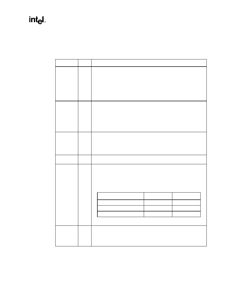
Table 52. Signal Definitions (Sheet 1 of 9)
Name
Type
Description
A[35:3]#
I/O
A[35:3]# (Address) define a 236 byte physical memory address space. In sub-phase
1 of the address phase, these pins transmit the address of a transaction. In sub-
phase 2, these pins transmit transaction type information. These signals must
connect the appropriate pins of all agents on the Intel Xeon processor MP on
the 0.13 micron process processor system bus. A[35:3]# are protected by parity
signals AP[1:0]#. A[35:3]# are source synchronous signals and are latched into the
receiving buffers by ADSTB[1:0]#.
On the active-to-inactive transition of RESET#, the processors sample a subset of
the A[35:3]# pins to determine their power-on configuration. See Section 6.1.
A20M#
I
If A20M# (Address-20 Mask) is asserted, the processor masks physical address bit
20 (A20#) before looking up a line in any internal cache and before driving a read/
write transaction on the bus. Asserting A20M# emulates the 8086 processor's
address wrap-around at the 1 MB boundary. Assertion of A20M# is only supported
in real mode.
A20M# is an asynchronous signal. However, to ensure recognition of this signal
following an I/O write instruction, it must be valid along with the TRDY# assertion of
the corresponding I/O write bus transaction.
ADS#
I/O
ADS# (Address Strobe) is asserted to indicate the validity of the transaction
address on the A[35:3]# pins. All bus agents observe the ADS# activation to begin
parity checking, protocol checking, address decode, internal snoop, or deferred
reply ID match operations associated with the new transaction. This signal must
connect the appropriate pins on all Intel Xeon processor MP on the 0.13 micron
process processor System Bus agents.
ADSTB[1:0]#
I/O
Address strobes are used to latch A[35:3]# and REQ[4:0]# on their rising and falling
edge.
AP[1:0]#
I/O
AP[1:0]# (Address Parity) are driven by the request initiator along with ADS#,
A[35:3]#, and the transaction type on the REQ[4:0]# pins. A correct parity signal is
high if an even number of covered signals are low and low if an odd number of
covered signals are low. This allows parity to be high when all the covered signals
are high. AP[1:0]# should connect the appropriate pins of all Intel Xeon processor
MP on the 0.13 micron process processor system bus agents. The following table
defines the coverage model of these signals.
BCLK[1:0]
I
The differential pair BCLK (Bus Clock) determines the bus frequency. All processor
system bus agents must receive these signals to drive their outputs and latch their
inputs.
All external timing parameters are specified with respect to the rising edge of
BCLK0 crossing the falling edge of BCLK1.
Request Signals
Subphase 1
Subphase 2
A[35:24]#
AP0#
AP1#
A[23:3]#
AP1#
AP0#
REQ[4:0]#
AP1#
AP0#
相關(guān)PDF資料 |
PDF描述 |
|---|---|
| BU-61582D0-290S | 2 CHANNEL(S), 1M bps, MIL-STD-1553 CONTROLLER, CQIP70 |
| BU-61582D0-300K | 2 CHANNEL(S), 1M bps, MIL-STD-1553 CONTROLLER, CQIP70 |
| BU-61582D1-391Q | 2 CHANNEL(S), 1M bps, MIL-STD-1553 CONTROLLER, CQIP70 |
| BU-61582D1-410S | 2 CHANNEL(S), 1M bps, MIL-STD-1553 CONTROLLER, CQIP70 |
| BU-61582D1-431 | 2 CHANNEL(S), 1M bps, MIL-STD-1553 CONTROLLER, CQIP70 |
相關(guān)代理商/技術(shù)參數(shù) |
參數(shù)描述 |
|---|---|
| BX80532KC2000D | 制造商:Intel 功能描述:MPU XEON PROCESSOR NETBURST 64-BIT 0.13UM 2GHZ - Boxed Product (Development Kits) |
| BX80532KC2000E | 制造商:Intel 功能描述:MPU XEON PROCESSOR NETBURST 64-BIT 0.13UM 2GHZ - Boxed Product (Development Kits) |
| BX80532KC2200DU | 制造商:Intel 功能描述:MPU XEON PROCESSOR NETBURST 64-BIT 0.13UM 2.2GHZ 603-PIN IN - Boxed Product (Development Kits) |
| BX80532KC2400D | 制造商:Intel 功能描述:MPU XEON PROCESSOR NETBURST 64-BIT 0.13UM 2.4GHZ - Boxed Product (Development Kits) |
| BX80532KC2400DU | 制造商:Intel 功能描述:MPU XEON PROCESSOR NETBURST 64-BIT 0.13UM 2.4GHZ - Boxed Product (Development Kits) |
發(fā)布緊急采購,3分鐘左右您將得到回復(fù)。