- 您現(xiàn)在的位置:買賣IC網(wǎng) > PDF目錄166447 > BN80C51FA-1 (INTEL CORP) 8-BIT, 16 MHz, MICROCONTROLLER, PQCC44 PDF資料下載
參數(shù)資料
| 型號(hào): | BN80C51FA-1 |
| 廠商: | INTEL CORP |
| 元件分類: | 微控制器/微處理器 |
| 英文描述: | 8-BIT, 16 MHz, MICROCONTROLLER, PQCC44 |
| 封裝: | PLASTIC, LCC-44 |
| 文件頁(yè)數(shù): | 12/13頁(yè) |
| 文件大?。?/td> | 1467K |
| 代理商: | BN80C51FA-1 |
第1頁(yè)第2頁(yè)第3頁(yè)第4頁(yè)第5頁(yè)第6頁(yè)第7頁(yè)第8頁(yè)第9頁(yè)第10頁(yè)第11頁(yè)當(dāng)前第12頁(yè)第13頁(yè)
AUTOMOTIVE 80C51FA/83C51FA
DC CHARACTERISTICS
: (TA eb40 Cto a125 C; VCC e 5V g10%; VSS e 0V) (Continued)
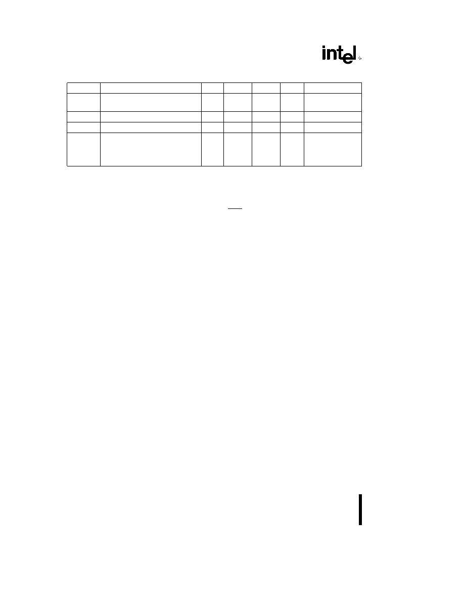
Symbol
Parameter
Min
Typ
Max
Unit
Test Conditions
ITL
Logical 1 to 0 Transition Current
b
265
b
650
m
AVIN e 2V
(Ports 1, 2, and 3)
RRST
RST Pulldown Resistor
40
100
225
KX
CIO
Pin Capacitance
10
pF
1MHz, 25 C
ICC
Power Supply Current:
(Note 3)
Running at 12 MHz (Figure 5)
40
mA
Idle Mode at 12 MHz (Figure 5)
15
mA
Power Down Mode (IPD)
150
m
A
NOTES
:
1. Capacitive loading on Ports 0 and 2 may cause noise pulses to be superimposed on the VOLs of ALE and Ports 1 and 3.
The noise is due to external bus capacitance discharging into the Port 0 and Port 2 pins when these pins make 1 to 0
transitions during bus operations. In applications where capacitance loading exceeds 100 pFs, the noise pulse on the ALE
signal may exceed 0.8V. In these cases, it may be desirable to qualify ALE with a Schmitt Trigger, or use an Address Latch
with a Schmitt Trigger Strobe input.
2. Capacitive loading on Ports 0 and 2 cause the VOH on ALE and PSEN to drop below the 0.9 VCC specification when the
address lines are stabilizing.
3. See Figures 6±9 for test conditions. Minimum VCC for Power Down is 2.0V.
4. Typicals are based on limited number of samples, and are not guaranteed. The values listed are at room temperature and
5.0V.
5. Under steady state (non-transient) conditions, IOL must be externally limited as follows:
Maximum IOL per Port Pin:
10 mA
Maximum IOL per 8-Bit Port -
Port 0:
26 mA
Ports 1, 2, and 3:
15 mA
Maximum Total IOL for all Output Pins:
71 mA
If IOL exceeds the test condition, VOL may exceed the related specification. Pins are not guaranteed to sink current greater
than the listed test conditions.
6. Contact Intel for design-in information.
8
相關(guān)PDF資料 |
PDF描述 |
|---|---|
| BPF-A410+ | 410 MHz, BAND PASS FILTER |
| BPW0484-10-07201-22AAAL | BGA484, IC SOCKET |
| BUW0484-10-07201-22AAA | BGA484, IC SOCKET |
| BUW484-1030-22AA01L | BGA484, IC SOCKET |
| BPW272-1270-20AC55 | BGA272, IC SOCKET |
相關(guān)代理商/技術(shù)參數(shù) |
參數(shù)描述 |
|---|---|
| BN-80H | 制造商:Taiyo Electric Ind. 功能描述: |
| BN8-12G08-03SD-Y70 | 制造商:Amphenol Corporation 功能描述:MIL-C-83723 FIREWALL - Bulk |
| BN8-12G12-12SD-Y70 | 制造商:Amphenol Corporation 功能描述:BN812G1212SDJ - Bulk |
| BN812G1624SDJ | 制造商:Amphenol Corporation 功能描述:MIL-C-83723 FIREWALL - Bulk |
| BN8-12G18-31SD-Y70 | 制造商:Amphenol Corporation 功能描述:MIL-C-83723 FIREWALL - Bulk |
發(fā)布緊急采購(gòu),3分鐘左右您將得到回復(fù)。