- 您現(xiàn)在的位置:買(mǎi)賣(mài)IC網(wǎng) > PDF目錄384114 > BA7242 (Rohm CO.,LTD.) Color TV signal encoder PDF資料下載
參數(shù)資料
| 型號(hào): | BA7242 |
| 廠商: | Rohm CO.,LTD. |
| 英文描述: | Color TV signal encoder |
| 中文描述: | 彩色電視信號(hào)編碼器 |
| 文件頁(yè)數(shù): | 2/5頁(yè) |
| 文件大小: | 61K |
| 代理商: | BA7242 |
2
Multimedia ICs
BA7242F
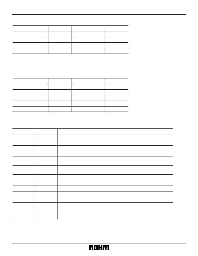
Absolute maximum ratings (Ta = 25°C)
Parameter
Symbol
Limits
7
450
– 20 ~ + 70
– 55 ~ + 125
Unit
V
mW
°
C
°
C
V
CC
Pd
Topr
Tstg
Power supply voltage
Power dissipation
Operating temperature
Storage temperature
Reduced by 4.5mW for each increase in Ta of 1
°
C over 25
°
C.
(When mounted on a 70mm
×
70mm
×
1.6mm glass epoxy board.)
Recommended operating conditions (Ta = 25°C)
Parameter
Symbol
Limits
4.5 ~ 5.5
0 ~ 0.7
0 ~ 0.7
0 ~ 0.7
0.45 ~ 0.60
Unit
V
V
P–P
V
P–P
V
P–P
V
P–P
V
CC
υ
RI
υ
GI
υ
BI
υ
SC
Power supply voltage
RIN input level
GIN input level
BIN input level
SCIN input level
Pin descriptions
Pin No.
1
Pin name
Function
BIN
Input for analog B signal. Operate with low impedance.
Input for analog G signal. Operate with low impedance.
Input for analog R signal. Operate with low impedance.
V
CC
for all except 75
driver.
Input for composite SYNC signal. Outputs SYNC signal to VOUT and YOUT pins
when input is LOW.
GND for all except 75
driver.
3.58MHz or 4.43MHz pulse signal input.
Video signal output mode setting. HIGH level = NTSC, LOW level = PAL.
Chrominance signal output. Internal 75
driver.
GND for 75
driver.
Composite video signal output. Internal 75
driver.
Luminance signal output. Internal 75
driver.
V
CC
for 75
driver.
2
GIN
3
RIN
4
V
CC
1
5
SYNC
6
BFP
7
GND1
8
SCIN
9
NT / PAL
10
C
OUT
11
GND2
12
V
OUT
13
Y
OUT
14
V
CC
2
Input for burst timing signal. Simultaneously performs the burst output and initiates
the pedestal clamp for the RIN, GIN, and BIN input signals when input is LOW.
相關(guān)PDF資料 |
PDF描述 |
|---|---|
| BA7274 | 4-channel video-signal PRE/REC amplifier |
| BA7356 | VIF/SIF SIGNAL PROCESSOR |
| BA7356S | VIF/SIF SIGNAL PROCESSOR |
| BA7357 | VIF / SIF signal processor |
| BA7605 | Video signal switcher |
相關(guān)代理商/技術(shù)參數(shù) |
參數(shù)描述 |
|---|---|
| BA7242F | 制造商:ROHM 制造商全稱(chēng):Rohm 功能描述:Color TV signal encoder |
| BA7244BS | 制造商:未知廠家 制造商全稱(chēng):未知廠家 功能描述:Consumer IC |
| BA7252S | 制造商:ROHM 制造商全稱(chēng):Rohm 功能描述:Switchless Video signal Playback/Record Amplifier |
| BA7253S | 制造商:未知廠家 制造商全稱(chēng):未知廠家 功能描述:Consumer IC |
| BA7254S | 制造商:未知廠家 制造商全稱(chēng):未知廠家 功能描述:Consumer IC |
發(fā)布緊急采購(gòu),3分鐘左右您將得到回復(fù)。