- 您現(xiàn)在的位置:買賣IC網(wǎng) > PDF目錄375384 > AX88772_07 (ASIX Electronics Corporation) USB to 10/100 Fast Ethernet/HomePNA Controller PDF資料下載
參數(shù)資料
| 型號: | AX88772_07 |
| 廠商: | ASIX Electronics Corporation |
| 英文描述: | USB to 10/100 Fast Ethernet/HomePNA Controller |
| 中文描述: | USB至10/100快速以太網(wǎng)/電話線網(wǎng)絡(luò)控制器 |
| 文件頁數(shù): | 19/43頁 |
| 文件大小: | 318K |
| 代理商: | AX88772_07 |
第1頁第2頁第3頁第4頁第5頁第6頁第7頁第8頁第9頁第10頁第11頁第12頁第13頁第14頁第15頁第16頁第17頁第18頁當(dāng)前第19頁第20頁第21頁第22頁第23頁第24頁第25頁第26頁第27頁第28頁第29頁第30頁第31頁第32頁第33頁第34頁第35頁第36頁第37頁第38頁第39頁第40頁第41頁第42頁第43頁
ASIX ELECTRONICS CORPORATION
19
AX88772
USB to 10/100 Fast Ethernet/HomePNA Controller
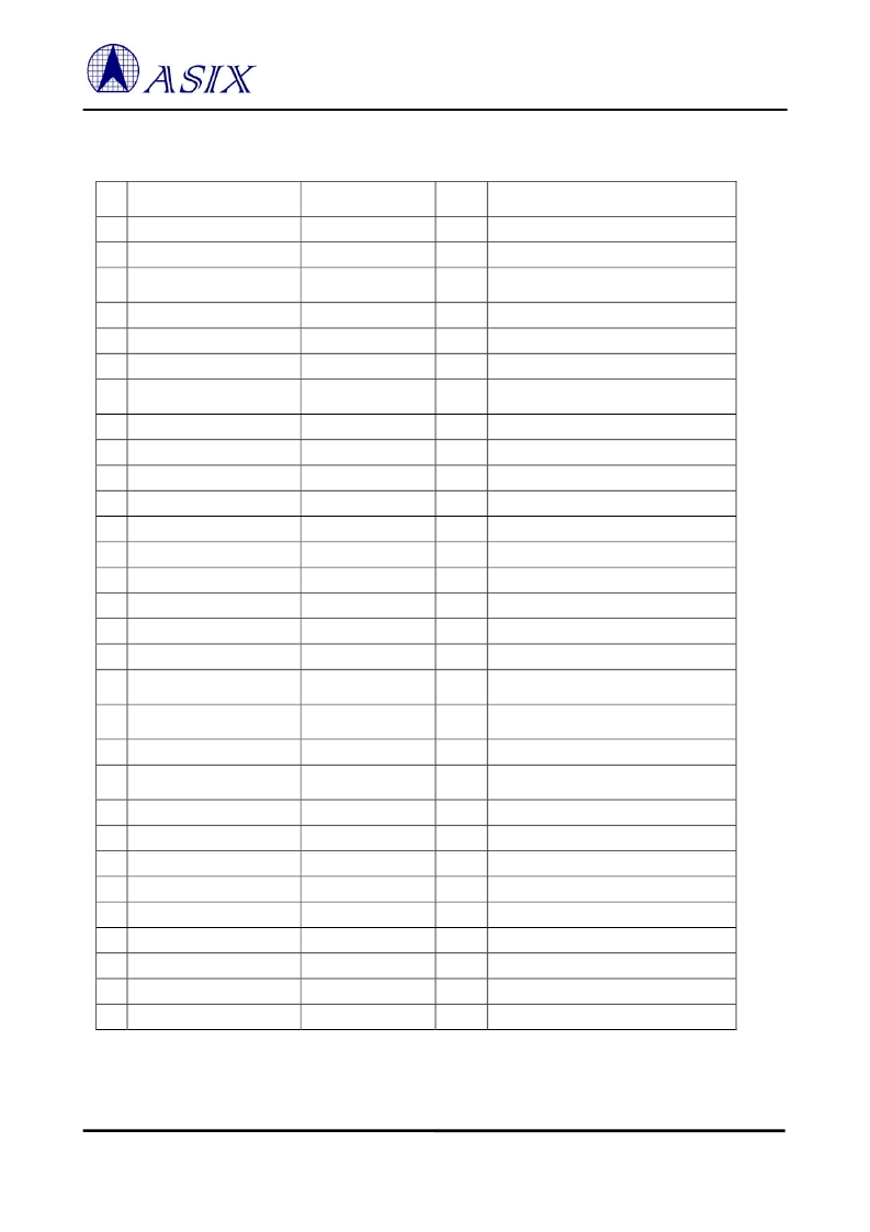
6.2 USB Vendor Commands
No
Setup Command
Data Bytes
Access
Type
Read Rx/Tx SRAM Read Register
Description
1. C002_AA0B_0C00_0800
8 bytes in Data stage
2. 4003_AA0B_0C00_0800
8 bytes in Data stage
Write Rx/Tx SRAM Write Register
3. 4006_0000_0000_0000
No data in Data stage
Write Software Serial Management Control
Register
Read PHY Read Register
4. C007_ AA00_CC00_0200 2 bytes in Data stage
5. 4008 _AA00_CC00_0200
2 bytes in Data stage
Write PHY Write Register
6. C009_0000_0000_0100
1 bytes in Data stage
Read Serial Management Status Register
7. 400A_0000_0000_0000
No data in Data stage
Write Hardware Serial Management Control
Register
Read SROM Read Register
8. C00B_AA00_0000_0200
2 bytes in Data stage
9. 400C_AA00_CCDD_0000 No data in Data stage
Write SROM Write Register
10. 400D_0000_0000_0000
No data in Data stage
Write SROM Write Enable Register
11. 400E_0000_0000_0000
No data in Data stage
Write SROM Write Disable Register
12. C00F_0000_0000_0200
2 bytes in Data stage
Read Rx Control Register
13. 4010_AABB_0000_0000
No data in Data stage
Write Rx Control Register
14. C011_0000_0000_0300
3 bytes in Data stage
Read IPG/IPG1/IPG2 Register
15. 4012_AABB_CC00_0000
No data in Data stage
Write IPG/IPG1/IPG2 Register
16. C013_0000_0000_0600
6 bytes in Data stage
Read Node ID Register
17. 4014_0000_0000_0600
6 bytes in Data stage
Write Node ID Register
18. C015_0000_0000_0800
8 bytes,
MA0~MA7
, in
Data stage
8 bytes,
MA0~MA7
, in
Data stage
No data in Data stage
Read Multicast Filter Array Register
19. 4016_0000_0000_0800
Write Multicast Filter Array Register
20. 4017_AA00_0000_0000
Write Test Register
21. C019_0000_0000_0200
2 bytes in Data stage
Read Ethernet/HomePNA Phy Address
Register
Read Medium Status Register
22. C01A_0000_0000_0200
2 bytes in Data stage
23. 401B_AABB_0000 _0000 No data in Data stage
Write Medium Mode Register
24. C01C_0000_0000_0100
1bytes in Data stage
Read Monitor Mode Status Register
25. 401D_AA00_0000_0000
No data in Data stage
Write Monitor Mode Register
26. C01E _0000_0000_0100
1 bytes in Data stage
Read GPIOs Status Register
27. 401F_AA00_0000_0000
No data in Data stage
Write GPIOs Register
28. 4020_AA00_0000_0000
No data in Data stage
Write Software Reset Register
29. C021_AA00_0000_0100
1 bytes in Data stage
Read Software PHY Select Status Register
30. 4022_AA00_0000_0000
No data in Data stage
Write Software PHY Select Register
Table 4: USB Vendor Command Register Map
相關(guān)PDF資料 |
PDF描述 |
|---|---|
| AX88772 | USB to 10/100 Fast Ethernet/HomePNA Controller |
| AX88780_07 | IC,D/A CONVERTER,MC144110DW, 6-BIT,5-15V,SOIC-20,3-7US SER. |
| AX88780 | High-Performance Non-PCI Single-Chip 32-bit 10/100M Fast Ethernet Controller |
| AX88790L | 10/100BASE 3-in-1 PCMCIA Fast Ethernet Controller |
| AX88796BLF | IC,MC14411P |
相關(guān)代理商/技術(shù)參數(shù) |
參數(shù)描述 |
|---|---|
| AX88772A | 制造商:ASIX 制造商全稱:ASIX 功能描述:USB 2.0 to 10/100M Fast Ethernet Controller |
| AX88772ALF | 制造商:ASIX Electronics Corporation 功能描述: |
| AX88772B | 制造商:ASIX 制造商全稱:ASIX 功能描述:AX88796C -- 低功耗 SPI或Non-PCI以太網(wǎng)控制器與方案 |
| AX88772BLF | 制造商:ASIX Electronics Corporation 功能描述: |
| AX88772BLI | 制造商:ASIX Electronics Corporation 功能描述: |
發(fā)布緊急采購,3分鐘左右您將得到回復(fù)。