- 您現(xiàn)在的位置:買賣IC網(wǎng) > PDF目錄4470 > AX250-FGG256 (Microsemi SoC)IC FPGA AXCELERATOR 250K 256FBGA PDF資料下載
參數(shù)資料
| 型號: | AX250-FGG256 |
| 廠商: | Microsemi SoC |
| 文件頁數(shù): | 191/262頁 |
| 文件大?。?/td> | 0K |
| 描述: | IC FPGA AXCELERATOR 250K 256FBGA |
| 標(biāo)準(zhǔn)包裝: | 90 |
| 系列: | Axcelerator |
| 邏輯元件/單元數(shù): | 2816 |
| RAM 位總計(jì): | 55296 |
| 輸入/輸出數(shù): | 138 |
| 門數(shù): | 250000 |
| 電源電壓: | 1.425 V ~ 1.575 V |
| 安裝類型: | 表面貼裝 |
| 工作溫度: | 0°C ~ 70°C |
| 封裝/外殼: | 256-LBGA |
| 供應(yīng)商設(shè)備封裝: | 256-FPBGA(17x17) |
第1頁第2頁第3頁第4頁第5頁第6頁第7頁第8頁第9頁第10頁第11頁第12頁第13頁第14頁第15頁第16頁第17頁第18頁第19頁第20頁第21頁第22頁第23頁第24頁第25頁第26頁第27頁第28頁第29頁第30頁第31頁第32頁第33頁第34頁第35頁第36頁第37頁第38頁第39頁第40頁第41頁第42頁第43頁第44頁第45頁第46頁第47頁第48頁第49頁第50頁第51頁第52頁第53頁第54頁第55頁第56頁第57頁第58頁第59頁第60頁第61頁第62頁第63頁第64頁第65頁第66頁第67頁第68頁第69頁第70頁第71頁第72頁第73頁第74頁第75頁第76頁第77頁第78頁第79頁第80頁第81頁第82頁第83頁第84頁第85頁第86頁第87頁第88頁第89頁第90頁第91頁第92頁第93頁第94頁第95頁第96頁第97頁第98頁第99頁第100頁第101頁第102頁第103頁第104頁第105頁第106頁第107頁第108頁第109頁第110頁第111頁第112頁第113頁第114頁第115頁第116頁第117頁第118頁第119頁第120頁第121頁第122頁第123頁第124頁第125頁第126頁第127頁第128頁第129頁第130頁第131頁第132頁第133頁第134頁第135頁第136頁第137頁第138頁第139頁第140頁第141頁第142頁第143頁第144頁第145頁第146頁第147頁第148頁第149頁第150頁第151頁第152頁第153頁第154頁第155頁第156頁第157頁第158頁第159頁第160頁第161頁第162頁第163頁第164頁第165頁第166頁第167頁第168頁第169頁第170頁第171頁第172頁第173頁第174頁第175頁第176頁第177頁第178頁第179頁第180頁第181頁第182頁第183頁第184頁第185頁第186頁第187頁第188頁第189頁第190頁當(dāng)前第191頁第192頁第193頁第194頁第195頁第196頁第197頁第198頁第199頁第200頁第201頁第202頁第203頁第204頁第205頁第206頁第207頁第208頁第209頁第210頁第211頁第212頁第213頁第214頁第215頁第216頁第217頁第218頁第219頁第220頁第221頁第222頁第223頁第224頁第225頁第226頁第227頁第228頁第229頁第230頁第231頁第232頁第233頁第234頁第235頁第236頁第237頁第238頁第239頁第240頁第241頁第242頁第243頁第244頁第245頁第246頁第247頁第248頁第249頁第250頁第251頁第252頁第253頁第254頁第255頁第256頁第257頁第258頁第259頁第260頁第261頁第262頁
Detailed Specifications
2- 20
R e v i sio n 1 8
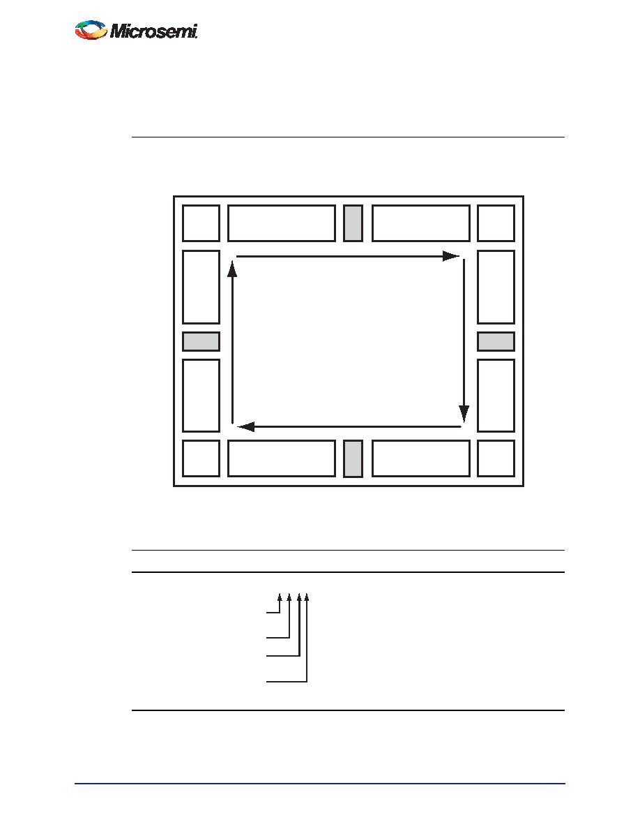
User I/O Naming Conventions
Due to the complex and flexible nature of the Axcelerator family’s user I/Os, a naming scheme is used to
show the details of the I/O. The naming scheme explains to which bank an I/O belongs, as well as the
pairing and pin polarity for differential I/Os (Figure 2-7).
Figure 2-7
I/O Bank and Dedicated Pin Layout
Figure 2-8
General Naming Schemes
PRC
PRD
Corner4
Corner3
Corner1
I/O
BANK
3
I/O
BANK
2
I/O BANK 0
I/O BANK 5
I/O BANK 1
I/O BANK 4
I/O
BANK
7
I/O
BANK
6
Corner2
AX125
GND
VCCDA
GND
VCCDA
VPUMP
GND
VCCDA
GND
VCCDA
VCOMPLG
VCOMPLH VCCPLG
VCCPLH
VCOMPLB
VCOMPLA
VCCPLB
VCCPLA
VCOMPLE
VCOMPLF VCCPLE
VCCPLF
VCOMPLD
VCOMPLC
VCCPLD
VCCPLC
GND
VCCDA
GND
VCCDA
GND
VCCDA
GND
VCCDA
GND
VCCA
GND
VCCA
GND
VCCA
GND
VCCA
GND
VCCA
GND
VCCA
GND
VCCI2
GND
VCCI1
GND
VCCI5
GND
VCCI4
GND
VCCDA
GND
VCCDA
GND
VCCDA
GND
VCCA
GND
VCCA
GND
VCCI6
GND
VCCI7
GND
VCCI3
VCCI0
PRB
PRA
TDO
TDI
TCK
TMS
TRST
LP
IOxxXBxFx
Fx refers to an
unimplemented feature
and can be ignored.
Bank I/D 0 through 7,
clockwise from IOB NW
P - Positive Pin/ N - Negative Pin
Pair number in the
bank, starting at 00,
clockwise from IOB NW
IO12PB1F1 is the positive pin of the thirteenth pair of the
first I/O bank (IOB NE). IO12PB1 combined
with IO12NB1 form a differential pair.
For those I/Os that can be employed
either as a user I/O or as a special
function, the following nomenclature
is used:
IOxxXBxFx/special_function_name
IOxxPB1Fx/xCLKx this pin can be configured as a clock
input or as a user I/O.
Examples:
發(fā)布緊急采購,3分鐘左右您將得到回復(fù)。