- 您現(xiàn)在的位置:買賣IC網(wǎng) > PDF目錄375378 > AU2903N (NXP SEMICONDUCTORS) Low power dual voltage comparator PDF資料下載
參數(shù)資料
| 型號(hào): | AU2903N |
| 廠商: | NXP SEMICONDUCTORS |
| 元件分類: | 運(yùn)動(dòng)控制電子 |
| 英文描述: | Low power dual voltage comparator |
| 中文描述: | DUAL COMPARATOR, 5000 uV OFFSET-MAX, 1300 ns RESPONSE TIME, PDIP8 |
| 封裝: | 0.300 INCH, PLASTIC, SOT-97-1, DIP-8 |
| 文件頁數(shù): | 3/5頁 |
| 文件大小: | 99K |
| 代理商: | AU2903N |
Philips Semiconductors Linear Products
Product specification
AU2903
Low power dual voltage comparator
August 31, 1994
302
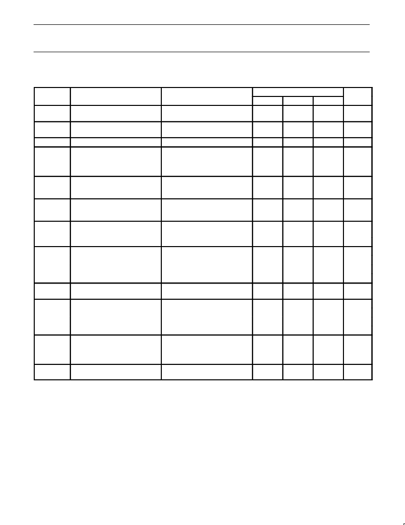
DC AND AC ELECTRICAL CHARACTERISTICS
V+=5V
DC
, AU2903; -40
°
C, T
A
≤
+125
°
C, unless otherwise specified.
SYMBOL
PARAMETER
TEST CONDITIONS
AU2903
Typ
±
2.0
±
9
UNIT
Min
Max
±
7.0
±
15
V
OS
Input offset voltage
2
T
A
= 25
°
C
Over temp.
mV
V
CM
Input common-mode voltage
range
3, 6
Differential input voltage
1
T
A
= 25
°
C
Over temp.
0
0
V+-1.5
V+-2.0
V
V
IDR
Keep all V
IN
s
≥
0V
DC
(or V- if need)
I
IN(+)
or I
IN(-)
with output
in linear range
T
A
=25
°
C
Over temp.
V+
V
I
BIAS
Input bias current
4
25
200
250
500
nA
I
OS
Input offset current
I
IN(+)
- I
IN(-)
T
A
= 25
°
C
Over temp.
±
5
±
50
±
50
±
200
nA
nA
I
OL
Output sink current
V
IN(-)
≥
1V
DC
, V
IN(+)
= 0,
V
0
≤
1.5V
DC
T
A
= 25
°
C
V
IN(+)
≥
1V
DC
, V
IN(-)
= 0
V
0
= 5V
DC
, T
A
= 25
°
C
V
0
= 30V
DC
, over temp.
R
L
=
∞
on both
comparators.
T
A
= 25
°
C
V+ = 30V, over temp.
R
L
≥
15k
, V+ = 15V
DC
,
T
A
= 25
°
C
V
IN(-)
≥
1V
DC
, V
IN(+)
= 0,
I
SINK
≤
4mA
T
A
= 25
°
C
Over temp.
6.0
16
mA
I
OH
Output leakage current
0.1
nA
1.0
μ
A
I
CC
Supply current
0.8
1
mA
1
2.5
A
V
Voltage gain
25
100
V/mV
V
OL
Saturation voltage
400
400
mV
700
t
LSR
Large-signal
response time
V
IN
= TTL logic swing,
V
REF
= 1.4V
DC
V
RL
= 5V
DC
, R
L
= 5.1k
,
T
A
= 25
°
C
V
RL
= 5V
DC
, R
L
= 5.1k
T
A
= 25
°
C
300
ns
t
R
Response time
5
1.3
μ
s
NOTES:
1. Positive excursions of input voltage may exceed the power supply level by 17V. As long as the other voltage remains within the
common-mode range, the comparator will provide a proper output state. The low input voltage state must not be less than -0.3V
DC
(V
DC
below the magnitude of the negative power supply, if used).
2. At output switch point, V
O
≈
1.4V
DC
, R
S
= 0
with V+ from 5V
DC
to 30V
DC
and over the full input common-mode range (0V
DC
to
V+-1.5V
DC
).
3. The input common-mode voltage or either input signal voltage should not be allowed to go negative by more than 0.3V. The upper end of the
common-mode voltage range is V+-1.5V, but either or both inputs can go to 30V
DC
without damage.
4. The direction of the input current is out of the IC due to the PNP input stage. This current is essentially constant, independent of the state of
the output so no loading change exists on the reference or input lines.
5. The response time specified is for a 100mV input step with a 5mV overdrive.
6. For input signals that exceed V
, only the over-driven comparator is affected. With a 5V supply, V
IN
should be limited to 25V maximum,
and a limiting resistor should be used on all inputs that might exceed the positive supply.
相關(guān)PDF資料 |
PDF描述 |
|---|---|
| AU5232 | Matched dual high-performance low-voltage operational amplifier |
| AU5232D | Matched dual high-performance low-voltage operational amplifier |
| AU5232N | Matched dual high-performance low-voltage operational amplifier |
| AU5780 | SAE/J1850/VPW transceiver |
| AU5780A | SAE/J1850/VPW transceiver |
相關(guān)代理商/技術(shù)參數(shù) |
參數(shù)描述 |
|---|---|
| AU2904 | 制造商:PHILIPS 制造商全稱:NXP Semiconductors 功能描述:Low power dual operational amplifier |
| AU2904D | 制造商:PHILIPS 制造商全稱:NXP Semiconductors 功能描述:Low power dual operational amplifier |
| AU2904N | 制造商:PHILIPS 制造商全稱:NXP Semiconductors 功能描述:Low power dual operational amplifier |
| AU-2929 | 制造商:Greenlee Textron Inc 功能描述: |
| AU-2M-02 | 功能描述:工業(yè)繼電器 AUX. SWITCH FOR GMC/D-12M;FRONT MOUNT, 2NC RoHS:否 制造商:TE Connectivity / Kilovac 觸點(diǎn)形式:1 Form A (SPST-NO) 觸點(diǎn)電流額定值: 線圈電壓:9 VDC to 36 VDC 線圈電阻:38 Ohms 線圈電流: 切換電壓: 安裝風(fēng)格:Panel 觸點(diǎn)材料:Silver Palladium |
發(fā)布緊急采購,3分鐘左右您將得到回復(fù)。