- 您現(xiàn)在的位置:買賣IC網(wǎng) > PDF目錄4411 > APA450-FG144I (Microsemi SoC)IC FPGA PROASIC+ 450K 144-FBGA PDF資料下載
參數(shù)資料
| 型號: | APA450-FG144I |
| 廠商: | Microsemi SoC |
| 文件頁數(shù): | 90/178頁 |
| 文件大?。?/td> | 0K |
| 描述: | IC FPGA PROASIC+ 450K 144-FBGA |
| 標(biāo)準(zhǔn)包裝: | 160 |
| 系列: | ProASICPLUS |
| RAM 位總計: | 110592 |
| 輸入/輸出數(shù): | 100 |
| 門數(shù): | 450000 |
| 電源電壓: | 2.3 V ~ 2.7 V |
| 安裝類型: | 表面貼裝 |
| 工作溫度: | -40°C ~ 85°C |
| 封裝/外殼: | 144-LBGA |
| 供應(yīng)商設(shè)備封裝: | 144-FPBGA(13x13) |
第1頁第2頁第3頁第4頁第5頁第6頁第7頁第8頁第9頁第10頁第11頁第12頁第13頁第14頁第15頁第16頁第17頁第18頁第19頁第20頁第21頁第22頁第23頁第24頁第25頁第26頁第27頁第28頁第29頁第30頁第31頁第32頁第33頁第34頁第35頁第36頁第37頁第38頁第39頁第40頁第41頁第42頁第43頁第44頁第45頁第46頁第47頁第48頁第49頁第50頁第51頁第52頁第53頁第54頁第55頁第56頁第57頁第58頁第59頁第60頁第61頁第62頁第63頁第64頁第65頁第66頁第67頁第68頁第69頁第70頁第71頁第72頁第73頁第74頁第75頁第76頁第77頁第78頁第79頁第80頁第81頁第82頁第83頁第84頁第85頁第86頁第87頁第88頁第89頁當(dāng)前第90頁第91頁第92頁第93頁第94頁第95頁第96頁第97頁第98頁第99頁第100頁第101頁第102頁第103頁第104頁第105頁第106頁第107頁第108頁第109頁第110頁第111頁第112頁第113頁第114頁第115頁第116頁第117頁第118頁第119頁第120頁第121頁第122頁第123頁第124頁第125頁第126頁第127頁第128頁第129頁第130頁第131頁第132頁第133頁第134頁第135頁第136頁第137頁第138頁第139頁第140頁第141頁第142頁第143頁第144頁第145頁第146頁第147頁第148頁第149頁第150頁第151頁第152頁第153頁第154頁第155頁第156頁第157頁第158頁第159頁第160頁第161頁第162頁第163頁第164頁第165頁第166頁第167頁第168頁第169頁第170頁第171頁第172頁第173頁第174頁第175頁第176頁第177頁第178頁
ProASICPLUS Flash Family FPGAs
v5.9
2-9
The TAP controller receives two control inputs (TMS and
TCK) and generates control and clock signals for the rest
of the test logic architecture. On power-up, the TAP
controller enters the Test-Logic-Reset state. To guarantee
a reset of the controller from any of the possible states,
TMS must remain high for five TCK cycles. The TRST pin
may also be used to asynchronously place the TAP
controller in the Test-Logic-Reset state.
ProASICPLUS devices support three types of test data
registers: bypass, device identification, and boundary
scan. The bypass register is selected when no other
register needs to be accessed in a device. This speeds up
test data transfer to other devices in a test data path.
The 32-bit device identification register is a shift register
with four fields (lowest significant byte (LSB), ID number,
part number and version). The boundary-scan register
observes and controls the state of each I/O pin.
Each I/O cell has three boundary-scan register cells, each
with a serial-in, serial-out, parallel-in, and parallel-out
pin. The serial pins are used to serially connect all the
boundary-scan register cells in a device into a boundary-
scan register chain, which starts at the TDI pin and ends
at the TDO pin. The parallel ports are connected to the
internal core logic tile and the input, output, and control
ports of an I/O buffer to capture and load data into the
register to control or observe the logic state of each I/O.
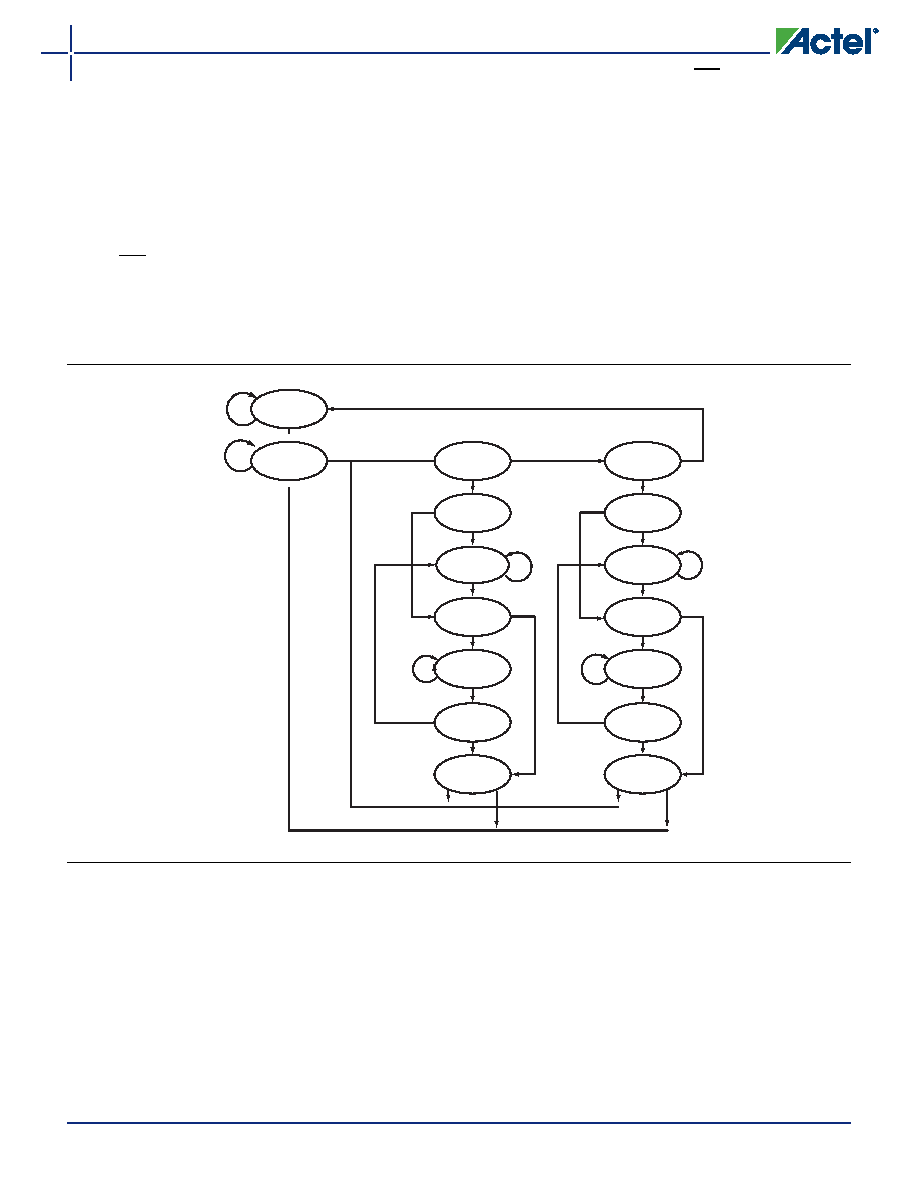
Figure 2-10 TAP Controller State Diagram
Test-Logic
Reset
Run-Test/
Idle
Select-DR-
Scan
Capture-DR
Shift-DR
Exit-DR
Pause-DR
Exit2-DR
Update-DR
Select-IR-
Scan
Capture-IR
Shift-IR
Exit-IR
Pause-IR
Exit2-IR
Update-IR
1
0
1
0
00
1
00
1
0
1
0
相關(guān)PDF資料 |
PDF描述 |
|---|---|
| AFS600-1FG484I | IC FPGA 4MB FLASH 600K 484FBGA |
| M1AFS600-1FGG484I | IC FPGA 4MB FLASH 600K 484-FBGA |
| M1AFS600-1FG484I | IC FPGA 4MB FLASH 600K 484-FBGA |
| AFS600-1FGG484I | IC FPGA 4MB FLASH 600K 484FBGA |
| 25AA160DT-I/MNY | IC SRL EEPROM 2KX8 1.8V 8-TDFN |
相關(guān)代理商/技術(shù)參數(shù) |
參數(shù)描述 |
|---|---|
| APA450-FG256 | 功能描述:IC FPGA PROASIC+ 450K 256-FBGA RoHS:否 類別:集成電路 (IC) >> 嵌入式 - FPGA(現(xiàn)場可編程門陣列) 系列:ProASICPLUS 產(chǎn)品培訓(xùn)模塊:Three Reasons to Use FPGA's in Industrial Designs Cyclone IV FPGA Family Overview 特色產(chǎn)品:Cyclone? IV FPGAs 標(biāo)準(zhǔn)包裝:60 系列:CYCLONE® IV GX LAB/CLB數(shù):9360 邏輯元件/單元數(shù):149760 RAM 位總計:6635520 輸入/輸出數(shù):270 門數(shù):- 電源電壓:1.16 V ~ 1.24 V 安裝類型:表面貼裝 工作溫度:0°C ~ 85°C 封裝/外殼:484-BGA 供應(yīng)商設(shè)備封裝:484-FBGA(23x23) |
| APA450-FG256A | 功能描述:IC FPGA PROASIC+ 450K 256-FBGA RoHS:否 類別:集成電路 (IC) >> 嵌入式 - FPGA(現(xiàn)場可編程門陣列) 系列:ProASICPLUS 產(chǎn)品培訓(xùn)模塊:Three Reasons to Use FPGA's in Industrial Designs Cyclone IV FPGA Family Overview 特色產(chǎn)品:Cyclone? IV FPGAs 標(biāo)準(zhǔn)包裝:60 系列:CYCLONE® IV GX LAB/CLB數(shù):9360 邏輯元件/單元數(shù):149760 RAM 位總計:6635520 輸入/輸出數(shù):270 門數(shù):- 電源電壓:1.16 V ~ 1.24 V 安裝類型:表面貼裝 工作溫度:0°C ~ 85°C 封裝/外殼:484-BGA 供應(yīng)商設(shè)備封裝:484-FBGA(23x23) |
| APA450-FG256I | 功能描述:IC FPGA PROASIC+ 450K 256-FBGA RoHS:否 類別:集成電路 (IC) >> 嵌入式 - FPGA(現(xiàn)場可編程門陣列) 系列:ProASICPLUS 產(chǎn)品培訓(xùn)模塊:Three Reasons to Use FPGA's in Industrial Designs Cyclone IV FPGA Family Overview 特色產(chǎn)品:Cyclone? IV FPGAs 標(biāo)準(zhǔn)包裝:60 系列:CYCLONE® IV GX LAB/CLB數(shù):9360 邏輯元件/單元數(shù):149760 RAM 位總計:6635520 輸入/輸出數(shù):270 門數(shù):- 電源電壓:1.16 V ~ 1.24 V 安裝類型:表面貼裝 工作溫度:0°C ~ 85°C 封裝/外殼:484-BGA 供應(yīng)商設(shè)備封裝:484-FBGA(23x23) |
| APA450-FG484 | 功能描述:IC FPGA PROASIC+ 450K 484-FBGA RoHS:否 類別:集成電路 (IC) >> 嵌入式 - FPGA(現(xiàn)場可編程門陣列) 系列:ProASICPLUS 產(chǎn)品培訓(xùn)模塊:Three Reasons to Use FPGA's in Industrial Designs Cyclone IV FPGA Family Overview 特色產(chǎn)品:Cyclone? IV FPGAs 標(biāo)準(zhǔn)包裝:60 系列:CYCLONE® IV GX LAB/CLB數(shù):9360 邏輯元件/單元數(shù):149760 RAM 位總計:6635520 輸入/輸出數(shù):270 門數(shù):- 電源電壓:1.16 V ~ 1.24 V 安裝類型:表面貼裝 工作溫度:0°C ~ 85°C 封裝/外殼:484-BGA 供應(yīng)商設(shè)備封裝:484-FBGA(23x23) |
| APA450-FG484A | 功能描述:IC FPGA PROASIC+ 450K 484-FBGA RoHS:否 類別:集成電路 (IC) >> 嵌入式 - FPGA(現(xiàn)場可編程門陣列) 系列:ProASICPLUS 產(chǎn)品培訓(xùn)模塊:Three Reasons to Use FPGA's in Industrial Designs Cyclone IV FPGA Family Overview 特色產(chǎn)品:Cyclone? IV FPGAs 標(biāo)準(zhǔn)包裝:60 系列:CYCLONE® IV GX LAB/CLB數(shù):9360 邏輯元件/單元數(shù):149760 RAM 位總計:6635520 輸入/輸出數(shù):270 門數(shù):- 電源電壓:1.16 V ~ 1.24 V 安裝類型:表面貼裝 工作溫度:0°C ~ 85°C 封裝/外殼:484-BGA 供應(yīng)商設(shè)備封裝:484-FBGA(23x23) |
發(fā)布緊急采購,3分鐘左右您將得到回復(fù)。