- 您現(xiàn)在的位置:買賣IC網(wǎng) > PDF目錄375330 > AND8020D (Analog Devices, Inc.) Termination of ECL Logic Devices with EF (Emitter Follower) OUTPUT Structure PDF資料下載
參數(shù)資料
| 型號(hào): | AND8020D |
| 廠商: | Analog Devices, Inc. |
| 英文描述: | Termination of ECL Logic Devices with EF (Emitter Follower) OUTPUT Structure |
| 中文描述: | ECL邏輯器件的終止與英法(發(fā)射極跟隨器)輸出結(jié)構(gòu) |
| 文件頁數(shù): | 16/18頁 |
| 文件大小: | 168K |
| 代理商: | AND8020D |
AND8020/D
http://onsemi.com
16
Figure 21. Differential and SingleEnded AC
Configurations Using V
BB
Reference
V
CC
or
V
TT
V
CC
Rpu 25 k to 100 k
Receiver
OUT
OUT
IN
INb
R
t
V
BB
V
TT
1 k
* 0.001 F
0.001 F
V
CC
or
V
TT
V
CC
Rpu 25 k to 100 k
Receiver
OUT
OUT
IN
V
BB
V
TT
1 k
* 0.001 F
0.01 0.001 F
R
t
R
t
R
t
* High Voltage Cap May Be Needed
0.01 0.001 F
A. Differential
B. SingleEnded
In Figure 21A, the IN line has a 1 k resistor to V
BB
,
presenting a 1 K impedance across the differential signal
lines. This assumes the signal impedance matching has been
accomplished prior to the cap coupling, on the driver side of
cap. Locate the coupling capacitor as physically close to the
input pin as possible to minimize the trace length and
diminish potential reflections due to the impedance
mismatch.
If signal impedance matching has not been accomplished
prior to the cap coupling, then a characteristic impedance
resistor, 2Z
0
, would be used across the input lines, on the
receiver side of the cap. The value of the Rpu resistor would
be adjusted to produce an acceptable null signal default
voltage drop.
AutoOscillation Suppression with V
BB
If the differential inputs to the AC coupled device are left
open or if the driving signals are lost, both receiver input pin
voltages converge toward the VBIAS reference voltage V
BB
value. Sustained oscillation may autonomously result from
a combination of ambient environmental noise, the device
small signal gain, and feedback from the output to the input
through parasitic capacitive and inductive paths.
As a differential receiver input voltage diverges, the
output responds by transitioning toward a state voltage. A
sufficient voltage across the receiver inputs will force the
output to state level. Depending on conditions, about 10 to
50 mV is sufficient to suppress instability oscillation and
force a determined state on the output.
For the configuration using the V
BB
reference, Figure 21,
this input voltage may be accomplished by injecting a
minimum current from V
CC
through an external pullup
resistor, Rpu, on ONE input line. The value of Rpu could
range from 25 k to 100 k . As Rpu increases, the phase
error is diminished and the susceptibility to oscillation
increases.
Generally, an internal pulldown resistor ranging in value
from 52 k to 75 k is deployed on an input pin. On some
Dbar (Invert) input pins an additional 36 k to 75 k
resistor is deployed to suppress oscillation by forcing a
determined state on the output under open input or null
voltage conditions. A minimum input voltage of 20 to
30 mV may be effective depending on noise, gain, and
layout.
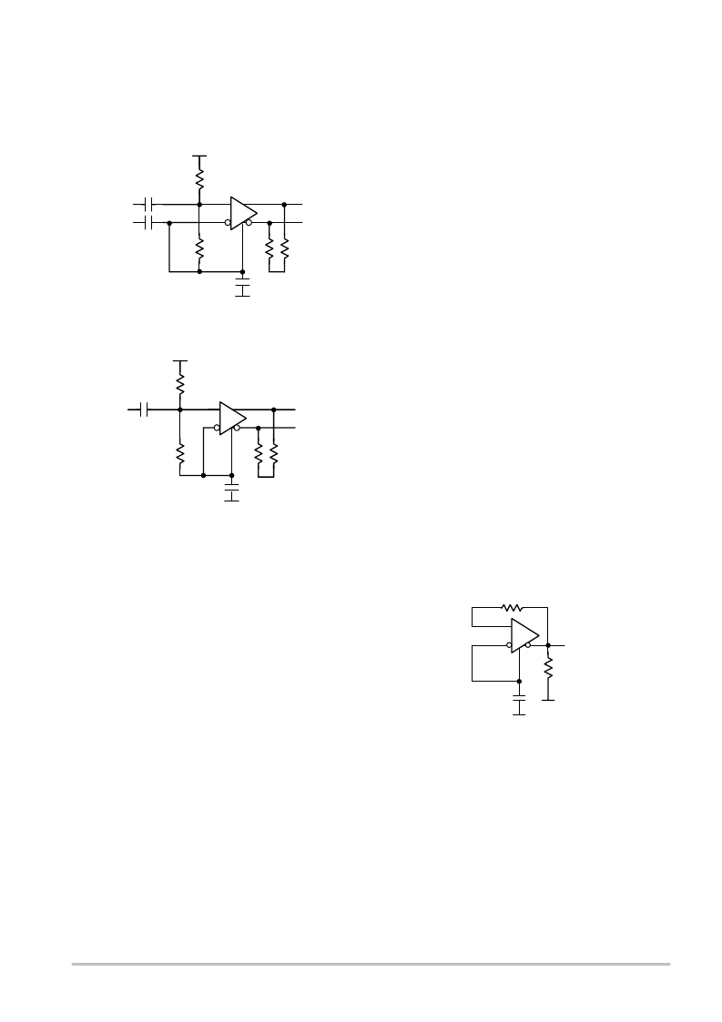
Generating V
BB
for VBIAS
When V
BB
voltages are desired, but not available within
a device, the reference level may be ported from a generator
as illustrated in Figure 22. Any of the “16” type buffers are
recommended for use in a high current gain V
BB
Generator
buffer. For example, the E416, EL16, LVEL16, EP16,
LVEP16, EL17, LVEL17, etc. type devices have a V
BB
pin
available for constructing a V
BB
Generator buffer.
Figure 22. V
BB
Voltage Reference Generator
V
BB(out)
16
RT
V
TT
V
CC
or V
TT
V
BB
0.01 F
1 K
NonV
BB
Biasing
Alternative to a device supplied V
BB
, any voltage source
may be supplied to bias receiver inputs to provide an
acceptable V
IHCMR
(Voltage Input HIGH Common Mode
Range) DC reference to the receiver (see specific device data
sheet). Signal impedance matching may be accomplished
prior to cap coupling, allowing a wide range values for a
rebiasing resistor network.
相關(guān)PDF資料 |
PDF描述 |
|---|---|
| ANP-C-115 | JT 79C 79#22D PIN RECP |
| ANPC-185 | GPS Antenna for Automotive Aftermarket Applications |
| AO3400 | N-Channel Enhancement Mode Field Effect Transistor |
| AO3400L | N-Channel Enhancement Mode Field Effect Transistor |
| AO3401A | P-Channel Enhancement Mode Field Effect Transistor |
相關(guān)代理商/技術(shù)參數(shù) |
參數(shù)描述 |
|---|---|
| AND8028 | 制造商:ONSEMI 制造商全稱:ON Semiconductor 功能描述:Precision Sub-One Volt 1.7 Ampere Output LDO |
| AND8028D | 制造商:ONSEMI 制造商全稱:ON Semiconductor 功能描述:Precision Sub-One Volt 1.7 Ampere Output LDO |
| AND8031 | 制造商:ONSEMI 制造商全稱:ON Semiconductor 功能描述:Isolated Precision Regulation of a Single 1.8 Volt Output from a Universal Line Input |
| AND8031D | 制造商:ONSEMI 制造商全稱:ON Semiconductor 功能描述:Isolated Precision Regulation of a Single 1.8 Volt Output from a Universal Line Input |
| AND8039 | 制造商:ONSEMI 制造商全稱:ON Semiconductor 功能描述:The One-Transistor Forward Converter |
發(fā)布緊急采購(gòu),3分鐘左右您將得到回復(fù)。