- 您現(xiàn)在的位置:買賣IC網(wǎng) > PDF目錄375326 > AN79N10 (PANASONIC CORP) PDF資料下載
參數(shù)資料
| 型號(hào): | AN79N10 |
| 廠商: | PANASONIC CORP |
| 元件分類: | 基準(zhǔn)電壓源/電流源 |
| 中文描述: | 10 V FIXED NEGATIVE REGULATOR, PSFM3 |
| 封裝: | TO-126, 3 PIN |
| 文件頁(yè)數(shù): | 8/9頁(yè) |
| 文件大?。?/td> | 63K |
| 代理商: | AN79N10 |
I
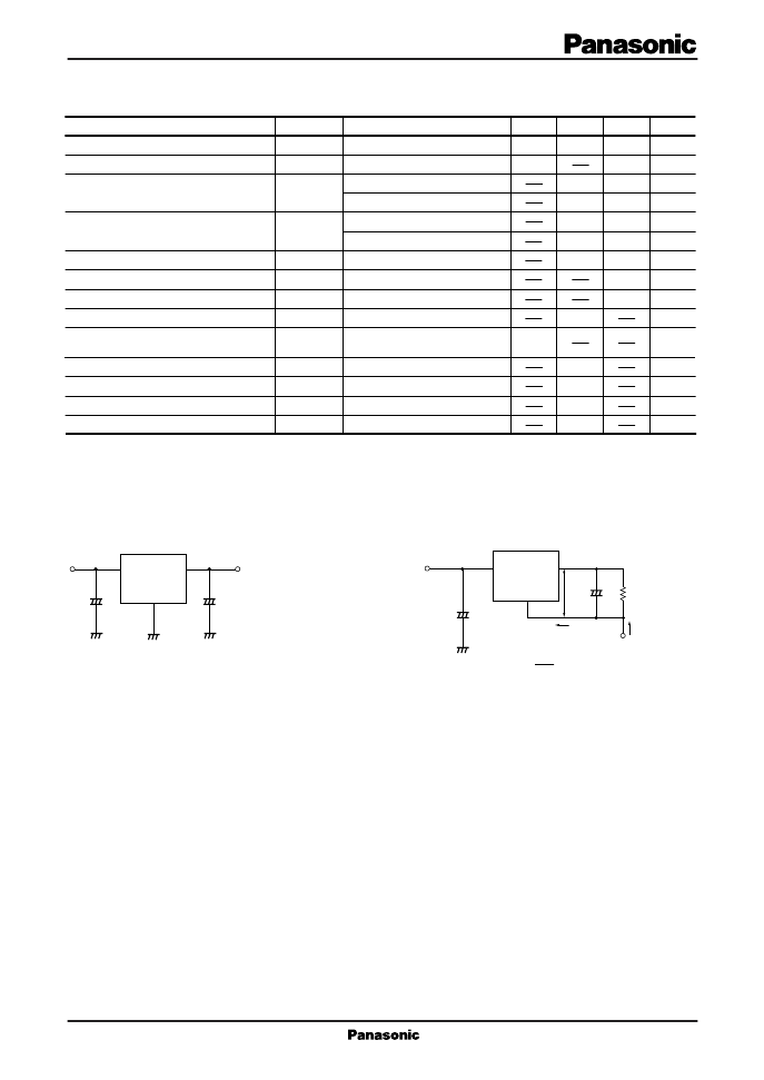
Basic Regulator Circuit
I
Application Circuit
T
j
=25C
V
I
=–
27 to –38V, I
O
=5 to 200mA
V
I
=–27 to –38V, T
j
=25C
V
I
=–27 to –37V, T
j
=25C
I
O
=1 to 300mA, T
j
=25C
I
O
=5 to 200mA, T
j
=25C
T
j
=25C
V
I
=–27 to –38V, T
j
=25C
I
O
=5 to 200mA, T
j
=25C
f=10Hz to 100kHz
V
=–28 to –38V, I
O
=50mA,
f=120Hz
I
O
=200mA, T
j
=25C
V
I
=–35V, T
j
=25C
T
j
=25C
I
O
=5mA
Note 1) The specified condition T
=25C means that the test should be carried out with the test time so short (within 10ms) that the
drift in characteristic value due to the rise in chip junction temperature can be ignored.
Note 2) When not specified, V
I
=–33V, I
O
=100mA, C
I
=2
μ
F, C
O
=1
μ
F and T
j
=0 to 125C
I
Bias (IN)
I
Bias (L)
V
no
μ
V
V
DIF (min.)
I
O (Short)
I
O (Peak)
V
O
/Ta
mV/C
I
Electrical Characteristics (Ta=25C)
·
AN79N24 (–24V Type)
Parameter
Output voltage
Output voltage tolerance
V
O
V
O
–25
–25.2
V
V
–24
REG
IN
80
70
mV
mV
mV
mV
mA
mA
mA
20
15
REG
L
30
10
3
I
Bias
600
dB
0.5
0.1
300
150
5
54
–23
–22.8
RR
V
1.1
mA
mA
10
500
–1
Symbol
Condition
min
typ
max
Unit
Line regulation
Load regulation
Bias current
Input bias current fluctuation
Load bias current fluctuation
Output noise voltage
Ripple rejection ratio
Minimum input/output voltage difference
Output short circuit current
Peak output current
Output voltage temperature coefficient
C
I
is connected when the input line is long. 2
μ
F
C
O
improves the transient response. 1
μ
F
O
–V
O
C
I
–V
I
Input
Output
AN79N00
Common
–
+
–
+
2
μ
F
I
Q
I
O
AN79N00
R
V
O
′
–V
I
|I
O
| = V
Q
O
′
1
μ
F
–
+
–
+
Common
Input
Output
相關(guān)PDF資料 |
PDF描述 |
|---|---|
| AN79N15 | |
| AN79N20 | |
| AN79N00SERIES | 3-pin Negative Output Voltage Regulator (300mA Type) |
| AN79N04 | |
| AN79N06 | |
相關(guān)代理商/技術(shù)參數(shù) |
參數(shù)描述 |
|---|---|
| AN79N12 | 制造商:Panasonic Industrial Company 功能描述:IC |
| AN79N15 | 制造商:PANASONIC 制造商全稱:Panasonic Semiconductor 功能描述: |
| AN79N18 | 制造商:未知廠家 制造商全稱:未知廠家 功能描述:Negative Fixed Voltage Regulator |
| AN79N20 | 制造商:PANASONIC 制造商全稱:Panasonic Semiconductor 功能描述: |
| AN79N24 | 制造商:未知廠家 制造商全稱:未知廠家 功能描述:Negative Fixed Voltage Regulator |
發(fā)布緊急采購(gòu),3分鐘左右您將得到回復(fù)。