- 您現(xiàn)在的位置:買賣IC網(wǎng) > PDF目錄375308 > AM49PDL127BH85IS (SPANSION LLC) 128 Megabit (8 M x 16-Bit) CMOS 3.0 Volt-only, Simultaneous Operation Flash Memory and 32 Mbit (2 M x 16-Bit) CMOS PDF資料下載
參數(shù)資料
| 型號: | AM49PDL127BH85IS |
| 廠商: | SPANSION LLC |
| 元件分類: | 存儲器 |
| 英文描述: | 128 Megabit (8 M x 16-Bit) CMOS 3.0 Volt-only, Simultaneous Operation Flash Memory and 32 Mbit (2 M x 16-Bit) CMOS |
| 中文描述: | SPECIALTY MEMORY CIRCUIT, PBGA73 |
| 封裝: | 8 X 11.60 MM, FBGA-73 |
| 文件頁數(shù): | 55/86頁 |
| 文件大小: | 588K |
| 代理商: | AM49PDL127BH85IS |
第1頁第2頁第3頁第4頁第5頁第6頁第7頁第8頁第9頁第10頁第11頁第12頁第13頁第14頁第15頁第16頁第17頁第18頁第19頁第20頁第21頁第22頁第23頁第24頁第25頁第26頁第27頁第28頁第29頁第30頁第31頁第32頁第33頁第34頁第35頁第36頁第37頁第38頁第39頁第40頁第41頁第42頁第43頁第44頁第45頁第46頁第47頁第48頁第49頁第50頁第51頁第52頁第53頁第54頁當前第55頁第56頁第57頁第58頁第59頁第60頁第61頁第62頁第63頁第64頁第65頁第66頁第67頁第68頁第69頁第70頁第71頁第72頁第73頁第74頁第75頁第76頁第77頁第78頁第79頁第80頁第81頁第82頁第83頁第84頁第85頁第86頁
December 16, 2003
Am49PDL127BH/Am49PDL129BH
53
A D V A N C E I N F O R M A T I O N
Legend:
DYB = Dynamic Protection Bit
OW = Address (A7:A0) is (00011010)
PD[3:0] = Password Data (1 of 4 portions)
PPB = Persistent Protection Bit
PWA = Password Address. A1:A0 selects portion of password.
PWD = Password Data being verified.
PL = Password Protection Mode Lock Address (A7:A0) is (00001010)
RD(0) = Read Data DQ0 for protection indicator bit.
RD(1) = Read Data DQ1 for PPB Lock status.
SA = Sector Address where security command applies. Address bits
A21:A12 uniquely select any sector.
SL = Persistent Protection Mode Lock Address (A7:A0) is (00010010)
WP = PPB Address (A7:A0) is (00000010) (Note 16)
X = Don’t care
PPMLB = Password Protection Mode Locking Bit
SPMLB = Persistent Protection Mode Locking Bit
1.
2.
3.
See Table 1 for description of bus operations.
All values are in hexadecimal.
Shaded cells in table denote read cycles. All other cycles are
write operations.
During unlock and command cycles, when lower address bits are
555 or 2AAh as shown in table, address bits higher than A11
(except where BA is required) and data bits higher than DQ7 are
don’t cares.
The reset command returns device to reading array.
Cycle 4 programs the addressed locking bit. Cycles 5 and 6
validate bit has been fully programmed when DQ0 = 1. If DQ0 = 0
in cycle 6, program command must be issued and verified again.
Data is latched on the rising edge of WE#.
Entire command sequence must be entered for each portion of
password.
Command sequence returns FFh if PPMLB is set.
4.
5.
6.
7.
8.
9.
10. The password is written over four consecutive cycles, at
addresses 0-3.
11. A 2 μs timeout is required between any two portions of password.
12. A 100 μs timeout is required between cycles 4 and 5.
13. A 1.2 ms timeout is required between cycles 4 and 5.
14. Cycle 4 erases all PPBs. Cycles 5 and 6 validate bits have been
fully erased when DQ0 = 0. If DQ0 = 1 in cycle 6, erase command
must be issued and verified again. Before issuing erase
command, all PPBs should be programmed to prevent PPB
overerasure.
15. DQ1 = 1 if PPB locked, 0 if unlocked.
16. For PDL128G and PDL640G, the WP address is 0111010. The
EP address (PPB Erase Address) is 1111010.
17. Following the final cycle of the command sequence, the user must
write the first three cycles of the Autoselect command and then
write a Reset command.
18. If checking the DYB status of sectors in multiple banks, the user
must follow Note 17 before crossing a bank boundary.
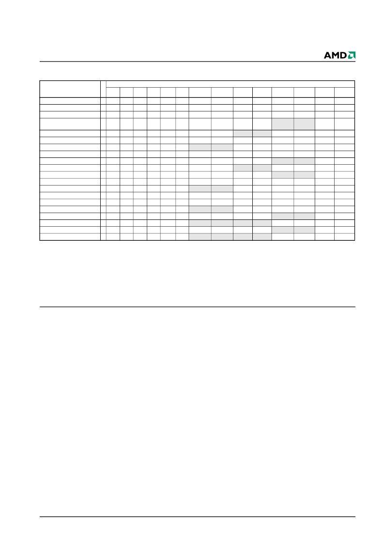
Table 16.
Sector Protection Command Definitions
Command (Notes)
C
1
3
4
Bus Cycles (Notes 1-4)
Addr Data Addr Data
Addr
Data
Addr
Data
Addr
Data
Addr
Data
Addr
Data
Reset
SecSi Sector Entry
SecSi Sector Exit
SecSi Protection Bit Program
(5, 6)
SecSi Protection Bit Status
Password Program (5, 7, 8)
Password Verify (6, 8, 9)
Password Unlock (7, 10, 11)
PPB Program (5, 6, 12, 17)
PPB Status
All PPB Erase (5, 6, 13, 14)
PPB Lock Bit Set (17)
PPB Lock Bit Status (15)
DYB Write (7)
DYB Erase (7)
DYB Status (6, 18)
PPMLB Program (5, 6, 12)
PPMLB Status (5)
SPMLB Program (5, 6, 12)
SPMLB Status (5)
XXX
555
555
F0
AA
AA
2AA
2AA
55
55
555
555
88
90
XX
00
6
555
AA
2AA
55
555
60
OW
68
OW
48
OW
RD(0)
5
4
4
7
6
5
6
3
4
4
4
4
6
5
6
5
555
555
555
555
555
555
555
555
555
555
555
555
555
555
555
555
AA
AA
AA
AA
AA
AA
AA
AA
AA
AA
AA
AA
AA
AA
AA
AA
2AA
2AA
2AA
2AA
2AA
2AA
2AA
2AA
2AA
2AA
2AA
2AA
2AA
2AA
2AA
2AA
55
55
55
55
55
55
55
55
55
55
55
55
55
55
55
55
555
555
555
555
555
555
555
555
555
555
555
555
555
555
555
555
60
38
C8
28
60
60
60
78
58
48
48
58
60
60
60
60
OW
XX[0-3]
PWA[0-3] PWD[0-3]
PWA[0]
(SA)WP
(SA)WP
WP
48
OW
RD(0)
PD[0-3]
PWD[0]
68
48
60
PWA[1]
(SA)WP
(SA)WP
(SA)
PWD[1]
48
RD (0)
40
PWA[2]
(SA)WP
PWD[2]
RD(0)
PWA[3]
PWD[3]
(SA)WP
RD(0)
SA
SA
SA
SA
PL
PL
SL
SL
RD(1)
X1
X0
RD(0)
68
48
68
48
PL
PL
SL
SL
48
PL
RD(0)
RD(0)
48
RD(0)
SL
RD(0)
相關PDF資料 |
PDF描述 |
|---|---|
| AM49PDL127BH85IT | 128 Megabit (8 M x 16-Bit) CMOS 3.0 Volt-only, Simultaneous Operation Flash Memory and 32 Mbit (2 M x 16-Bit) CMOS |
| AM49PDL129BH | 128 Megabit (8 M x 16-Bit) CMOS 3.0 Volt-only, Simultaneous Operation Flash Memory and 32 Mbit (2 M x 16-Bit) CMOS |
| AM49PDL129BH66IS | 128 Megabit (8 M x 16-Bit) CMOS 3.0 Volt-only, Simultaneous Operation Flash Memory and 32 Mbit (2 M x 16-Bit) CMOS |
| AM49PDL129BH66IT | 128 Megabit (8 M x 16-Bit) CMOS 3.0 Volt-only, Simultaneous Operation Flash Memory and 32 Mbit (2 M x 16-Bit) CMOS |
| AM49PDL129BH85IS | 128 Megabit (8 M x 16-Bit) CMOS 3.0 Volt-only, Simultaneous Operation Flash Memory and 32 Mbit (2 M x 16-Bit) CMOS |
相關代理商/技術參數(shù) |
參數(shù)描述 |
|---|---|
| AM49PDL127BH85IT | 制造商:SPANSION 制造商全稱:SPANSION 功能描述:128 Megabit (8 M x 16-Bit) CMOS 3.0 Volt-only, Simultaneous Operation Flash Memory and 32 Mbit (2 M x 16-Bit) CMOS |
| AM49PDL129AH | 制造商:SPANSION 制造商全稱:SPANSION 功能描述:128 Megabit (8 M x 16-Bit) CMOS 3.0 Volt-only, Simultaneous Operation Flash Memory and 16 Mbit (1 M x 16-Bit) CMOS Pseudo Static RAM |
| AM49PDL129AH61IS | 制造商:SPANSION 制造商全稱:SPANSION 功能描述:128 Megabit (8 M x 16-Bit) CMOS 3.0 Volt-only, Simultaneous Operation Flash Memory and 16 Mbit (1 M x 16-Bit) CMOS Pseudo Static RAM |
| AM49PDL129AH61IT | 制造商:SPANSION 制造商全稱:SPANSION 功能描述:128 Megabit (8 M x 16-Bit) CMOS 3.0 Volt-only, Simultaneous Operation Flash Memory and 16 Mbit (1 M x 16-Bit) CMOS Pseudo Static RAM |
| AM49PDL129AH70IS | 制造商:SPANSION 制造商全稱:SPANSION 功能描述:128 Megabit (8 M x 16-Bit) CMOS 3.0 Volt-only, Simultaneous Operation Flash Memory and 16 Mbit (1 M x 16-Bit) CMOS Pseudo Static RAM |
發(fā)布緊急采購,3分鐘左右您將得到回復。