- 鎮ㄧ従(xi脿n)鍦ㄧ殑浣嶇疆锛�璨疯常IC缍�(w菐ng) > PDF鐩寗4517 > AGL250V2-VQG100I (Microsemi SoC)IC FPGA 1KB FLASH 250K 100VQFP PDF璩囨枡涓嬭級
鍙冩暩(sh霉)璩囨枡
| 鍨嬭櫉锛� | AGL250V2-VQG100I |
| 寤犲晢锛� | Microsemi SoC |
| 鏂囦欢闋佹暩(sh霉)锛� | 246/250闋� |
| 鏂囦欢澶�?銆�?/td> | 0K |
| 鎻忚堪锛� | IC FPGA 1KB FLASH 250K 100VQFP |
| 妯�(bi膩o)婧�(zh菙n)鍖呰锛� | 90 |
| 绯诲垪锛� | IGLOO |
| 閭忚集鍏冧欢/鍠厓鏁�(sh霉)锛� | 6144 |
| RAM 浣嶇附瑷�(j矛)锛� | 36864 |
| 杓稿叆/杓稿嚭鏁�(sh霉)锛� | 68 |
| 闁€鏁�(sh霉)锛� | 250000 |
| 闆绘簮闆诲锛� | 1.14 V ~ 1.575 V |
| 瀹夎椤炲瀷锛� | 琛ㄩ潰璨艰 |
| 宸ヤ綔婧害锛� | -40°C ~ 85°C |
| 灏佽/澶栨锛� | 100-TQFP |
| 渚涙噳(y墨ng)鍟嗚ō(sh猫)鍌欏皝瑁濓細 | 100-VQFP锛�14x14锛� |
绗�1闋�绗�2闋�绗�3闋�绗�4闋�绗�5闋�绗�6闋�绗�7闋�绗�8闋�绗�9闋�绗�10闋�绗�11闋�绗�12闋�绗�13闋�绗�14闋�绗�15闋�绗�16闋�绗�17闋�绗�18闋�绗�19闋�绗�20闋�绗�21闋�绗�22闋�绗�23闋�绗�24闋�绗�25闋�绗�26闋�绗�27闋�绗�28闋�绗�29闋�绗�30闋�绗�31闋�绗�32闋�绗�33闋�绗�34闋�绗�35闋�绗�36闋�绗�37闋�绗�38闋�绗�39闋�绗�40闋�绗�41闋�绗�42闋�绗�43闋�绗�44闋�绗�45闋�绗�46闋�绗�47闋�绗�48闋�绗�49闋�绗�50闋�绗�51闋�绗�52闋�绗�53闋�绗�54闋�绗�55闋�绗�56闋�绗�57闋�绗�58闋�绗�59闋�绗�60闋�绗�61闋�绗�62闋�绗�63闋�绗�64闋�绗�65闋�绗�66闋�绗�67闋�绗�68闋�绗�69闋�绗�70闋�绗�71闋�绗�72闋�绗�73闋�绗�74闋�绗�75闋�绗�76闋�绗�77闋�绗�78闋�绗�79闋�绗�80闋�绗�81闋�绗�82闋�绗�83闋�绗�84闋�绗�85闋�绗�86闋�绗�87闋�绗�88闋�绗�89闋�绗�90闋�绗�91闋�绗�92闋�绗�93闋�绗�94闋�绗�95闋�绗�96闋�绗�97闋�绗�98闋�绗�99闋�绗�100闋�绗�101闋�绗�102闋�绗�103闋�绗�104闋�绗�105闋�绗�106闋�绗�107闋�绗�108闋�绗�109闋�绗�110闋�绗�111闋�绗�112闋�绗�113闋�绗�114闋�绗�115闋�绗�116闋�绗�117闋�绗�118闋�绗�119闋�绗�120闋�绗�121闋�绗�122闋�绗�123闋�绗�124闋�绗�125闋�绗�126闋�绗�127闋�绗�128闋�绗�129闋�绗�130闋�绗�131闋�绗�132闋�绗�133闋�绗�134闋�绗�135闋�绗�136闋�绗�137闋�绗�138闋�绗�139闋�绗�140闋�绗�141闋�绗�142闋�绗�143闋�绗�144闋�绗�145闋�绗�146闋�绗�147闋�绗�148闋�绗�149闋�绗�150闋�绗�151闋�绗�152闋�绗�153闋�绗�154闋�绗�155闋�绗�156闋�绗�157闋�绗�158闋�绗�159闋�绗�160闋�绗�161闋�绗�162闋�绗�163闋�绗�164闋�绗�165闋�绗�166闋�绗�167闋�绗�168闋�绗�169闋�绗�170闋�绗�171闋�绗�172闋�绗�173闋�绗�174闋�绗�175闋�绗�176闋�绗�177闋�绗�178闋�绗�179闋�绗�180闋�绗�181闋�绗�182闋�绗�183闋�绗�184闋�绗�185闋�绗�186闋�绗�187闋�绗�188闋�绗�189闋�绗�190闋�绗�191闋�绗�192闋�绗�193闋�绗�194闋�绗�195闋�绗�196闋�绗�197闋�绗�198闋�绗�199闋�绗�200闋�绗�201闋�绗�202闋�绗�203闋�绗�204闋�绗�205闋�绗�206闋�绗�207闋�绗�208闋�绗�209闋�绗�210闋�绗�211闋�绗�212闋�绗�213闋�绗�214闋�绗�215闋�绗�216闋�绗�217闋�绗�218闋�绗�219闋�绗�220闋�绗�221闋�绗�222闋�绗�223闋�绗�224闋�绗�225闋�绗�226闋�绗�227闋�绗�228闋�绗�229闋�绗�230闋�绗�231闋�绗�232闋�绗�233闋�绗�234闋�绗�235闋�绗�236闋�绗�237闋�绗�238闋�绗�239闋�绗�240闋�绗�241闋�绗�242闋�绗�243闋�绗�244闋�绗�245闋�鐣�(d膩ng)鍓嶇246闋�绗�247闋�绗�248闋�绗�249闋�绗�250闋�
IGLOO Low Power Flash FPGAs
Revision 23
2-79
1.2 V DC Core Voltage
Differential I/O Characteristics
Physical Implementation
Configuration of the I/O modules as a differential pair is handled by Microsemi Designer software when
the user instantiates a differential I/O macro in the design.
Differential I/Os can also be used in conjunction with the embedded Input Register (InReg), Output
Register (OutReg), Enable Register (EnReg), and Double Data Rate (DDR). However, there is no
support for bidirectional I/Os or tristates with the LVPECL standards.
LVDS
Low-Voltage Differential Signaling (ANSI/TIA/EIA-644) is a high-speed, differential I/O standard. It
requires that one data bit be carried through two signal lines, so two pins are needed. It also requires
external resistor termination.
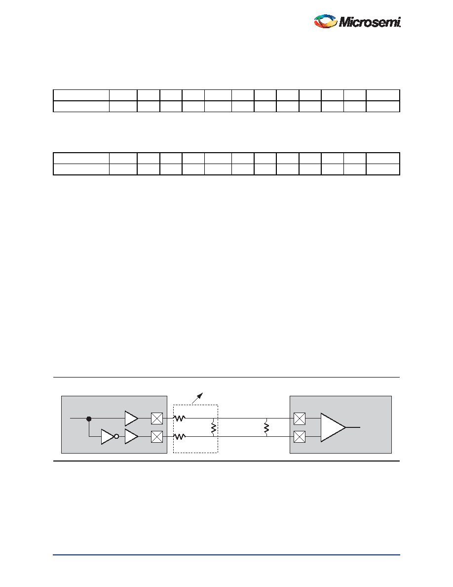
The full implementation of the LVDS transmitter and receiver is shown in an example in Figure 2-13. The
building blocks of the LVDS transmitter-receiver are one transmitter macro, one receiver macro, three
board resistors at the transmitter end, and one resistor at the receiver end. The values for the three driver
resistors are different from those used in the LVPECL implementation because the output standard
specifications are different.
Along with LVDS I/O, IGLOO also supports Bus LVDS structure and Multipoint LVDS (M-LVDS)
configuration (up to 40 nodes).
Table 2-145 3.3 V PCI/PCI-X
Commercial-Case Conditions: TJ = 70掳C, Worst-Case VCC = 1.14 V, Worst-Case VCCI = 3.0 V
Applicable to Advanced I/O Banks
Speed Grade
tDOUT
tDP
tDIN
tPY
tEOUT
tZL
tZH
tLZ
tHZ
tZLS
tZHS
Units
Std.
1.55
2.91
0.25
0.86
1.10
2.95
2.29
3.25
3.93
8.74
8.08
ns
Note: For specific junction temperature and voltage supply levels, refer to Table 2-7 on page 2-7 for derating values.
Table 2-146 3.3 V PCI/PCI-X
Commercial-Case Conditions: TJ = 70掳C, Worst-Case VCC = 1.14 V, Worst-Case VCCI = 3.0 V
Applicable to Standard Plus I/O Banks
Speed Grade
tDOUT
tDP
tDIN
tPY
tEOUT
tZL
tZH
tLZ
tHZ
tZLS
tZHS
Units
Std.
1.55
2.53
0.25
0.85
1.10
2.57
1.98
2.93
3.64
8.35
7.76
ns
Note: For specific junction temperature and voltage supply levels, refer to Table 2-7 on page 2-7 for derating values.
Figure 2-13 LVDS Circuit Diagram and Board-Level Implementation
140
100
Z0 = 50
165
165
+
鈥�
P
N
P
N
INBUF_LVDS
OUTBUF_LVDS
FPGA
Bourns Part Number: CAT16-LV4F12
鐩搁棞(gu膩n)PDF璩囨枡 |
PDF鎻忚堪 |
|---|---|
| AGL250V2-VQ100I | IC FPGA 1KB FLASH 250K 100VQFP |
| A3P250L-1FG144 | IC FPGA 1KB FLASH 250K 144-FBGA |
| A3P250L-1FGG144 | IC FPGA 1KB FLASH 250K 144-FBGA |
| EPF8282ATC100-3 | IC FLEX 8000A FPGA 2.5K 100-TQFP |
| GMC61DRSN-S273 | CONN EDGECARD 122PS DIP .100 SLD |
鐩搁棞(gu膩n)浠g悊鍟�/鎶€琛�(sh霉)鍙冩暩(sh霉) |
鍙冩暩(sh霉)鎻忚堪 |
|---|---|
| AGL250V2-VQG100IX399 | 鍒堕€犲晢:Microsemi Corporation 鍔熻兘鎻忚堪:FPGA IGLOO 250K GATES IND 130NM 1.2V/1.5V 100VQFP GOLD WIRE - Trays |
| AGL250V2-VQG100T | 鍒堕€犲晢:Microsemi Corporation 鍔熻兘鎻忚堪:AGL250V2-VQG100T - Trays 鍒堕€犲晢:Microsemi Corporation 鍔熻兘鎻忚堪:IC FPGA 68 I/O 100VQFP |
| AGL250V2-VQG144 | 鍒堕€犲晢:ACTEL 鍒堕€犲晢鍏ㄧū:Actel Corporation 鍔熻兘鎻忚堪:IGLOO Low-Power Flash FPGAs with Flash Freeze Technology |
| AGL250V2-VQG144ES | 鍒堕€犲晢:ACTEL 鍒堕€犲晢鍏ㄧū:Actel Corporation 鍔熻兘鎻忚堪:IGLOO Low-Power Flash FPGAs with Flash Freeze Technology |
| AGL250V2-VQG144I | 鍒堕€犲晢:ACTEL 鍒堕€犲晢鍏ㄧū:Actel Corporation 鍔熻兘鎻忚堪:IGLOO Low-Power Flash FPGAs with Flash Freeze Technology |
鐧�(f膩)甯冪穵鎬ラ噰璩�锛�3鍒嗛悩宸﹀彸鎮ㄥ皣寰楀埌鍥炲京(f霉)銆�
