- 您現(xiàn)在的位置:買(mǎi)賣(mài)IC網(wǎng) > PDF目錄4365 > AFS1500-2FGG676I (Microsemi SoC)IC FPGA 8MB FLASH 1.5M 676-FBGA PDF資料下載
第1頁(yè)第2頁(yè)第3頁(yè)第4頁(yè)第5頁(yè)第6頁(yè)第7頁(yè)第8頁(yè)第9頁(yè)第10頁(yè)第11頁(yè)第12頁(yè)第13頁(yè)第14頁(yè)第15頁(yè)第16頁(yè)第17頁(yè)第18頁(yè)第19頁(yè)第20頁(yè)第21頁(yè)第22頁(yè)第23頁(yè)第24頁(yè)第25頁(yè)第26頁(yè)第27頁(yè)第28頁(yè)第29頁(yè)第30頁(yè)第31頁(yè)第32頁(yè)第33頁(yè)第34頁(yè)第35頁(yè)第36頁(yè)第37頁(yè)第38頁(yè)第39頁(yè)第40頁(yè)第41頁(yè)第42頁(yè)第43頁(yè)第44頁(yè)第45頁(yè)第46頁(yè)第47頁(yè)第48頁(yè)第49頁(yè)第50頁(yè)第51頁(yè)第52頁(yè)第53頁(yè)第54頁(yè)第55頁(yè)第56頁(yè)第57頁(yè)第58頁(yè)第59頁(yè)第60頁(yè)第61頁(yè)第62頁(yè)第63頁(yè)第64頁(yè)第65頁(yè)第66頁(yè)第67頁(yè)第68頁(yè)第69頁(yè)第70頁(yè)第71頁(yè)第72頁(yè)第73頁(yè)第74頁(yè)第75頁(yè)第76頁(yè)第77頁(yè)第78頁(yè)第79頁(yè)第80頁(yè)第81頁(yè)第82頁(yè)第83頁(yè)第84頁(yè)第85頁(yè)第86頁(yè)第87頁(yè)第88頁(yè)第89頁(yè)第90頁(yè)第91頁(yè)第92頁(yè)第93頁(yè)第94頁(yè)第95頁(yè)第96頁(yè)第97頁(yè)第98頁(yè)第99頁(yè)第100頁(yè)第101頁(yè)第102頁(yè)第103頁(yè)第104頁(yè)第105頁(yè)當(dāng)前第106頁(yè)第107頁(yè)第108頁(yè)第109頁(yè)第110頁(yè)第111頁(yè)第112頁(yè)第113頁(yè)第114頁(yè)第115頁(yè)第116頁(yè)第117頁(yè)第118頁(yè)第119頁(yè)第120頁(yè)第121頁(yè)第122頁(yè)第123頁(yè)第124頁(yè)第125頁(yè)第126頁(yè)第127頁(yè)第128頁(yè)第129頁(yè)第130頁(yè)第131頁(yè)第132頁(yè)第133頁(yè)第134頁(yè)第135頁(yè)第136頁(yè)第137頁(yè)第138頁(yè)第139頁(yè)第140頁(yè)第141頁(yè)第142頁(yè)第143頁(yè)第144頁(yè)第145頁(yè)第146頁(yè)第147頁(yè)第148頁(yè)第149頁(yè)第150頁(yè)第151頁(yè)第152頁(yè)第153頁(yè)第154頁(yè)第155頁(yè)第156頁(yè)第157頁(yè)第158頁(yè)第159頁(yè)第160頁(yè)第161頁(yè)第162頁(yè)第163頁(yè)第164頁(yè)第165頁(yè)第166頁(yè)第167頁(yè)第168頁(yè)第169頁(yè)第170頁(yè)第171頁(yè)第172頁(yè)第173頁(yè)第174頁(yè)第175頁(yè)第176頁(yè)第177頁(yè)第178頁(yè)第179頁(yè)第180頁(yè)第181頁(yè)第182頁(yè)第183頁(yè)第184頁(yè)第185頁(yè)第186頁(yè)第187頁(yè)第188頁(yè)第189頁(yè)第190頁(yè)第191頁(yè)第192頁(yè)第193頁(yè)第194頁(yè)第195頁(yè)第196頁(yè)第197頁(yè)第198頁(yè)第199頁(yè)第200頁(yè)第201頁(yè)第202頁(yè)第203頁(yè)第204頁(yè)第205頁(yè)第206頁(yè)第207頁(yè)第208頁(yè)第209頁(yè)第210頁(yè)第211頁(yè)第212頁(yè)第213頁(yè)第214頁(yè)第215頁(yè)第216頁(yè)第217頁(yè)第218頁(yè)第219頁(yè)第220頁(yè)第221頁(yè)第222頁(yè)第223頁(yè)第224頁(yè)第225頁(yè)第226頁(yè)第227頁(yè)第228頁(yè)第229頁(yè)第230頁(yè)第231頁(yè)第232頁(yè)第233頁(yè)第234頁(yè)第235頁(yè)第236頁(yè)第237頁(yè)第238頁(yè)第239頁(yè)第240頁(yè)第241頁(yè)第242頁(yè)第243頁(yè)第244頁(yè)第245頁(yè)第246頁(yè)第247頁(yè)第248頁(yè)第249頁(yè)第250頁(yè)第251頁(yè)第252頁(yè)第253頁(yè)第254頁(yè)第255頁(yè)第256頁(yè)第257頁(yè)第258頁(yè)第259頁(yè)第260頁(yè)第261頁(yè)第262頁(yè)第263頁(yè)第264頁(yè)第265頁(yè)第266頁(yè)第267頁(yè)第268頁(yè)第269頁(yè)第270頁(yè)第271頁(yè)第272頁(yè)第273頁(yè)第274頁(yè)第275頁(yè)第276頁(yè)第277頁(yè)第278頁(yè)第279頁(yè)第280頁(yè)第281頁(yè)第282頁(yè)第283頁(yè)第284頁(yè)第285頁(yè)第286頁(yè)第287頁(yè)第288頁(yè)第289頁(yè)第290頁(yè)第291頁(yè)第292頁(yè)第293頁(yè)第294頁(yè)第295頁(yè)第296頁(yè)第297頁(yè)第298頁(yè)第299頁(yè)第300頁(yè)第301頁(yè)第302頁(yè)第303頁(yè)第304頁(yè)第305頁(yè)第306頁(yè)第307頁(yè)第308頁(yè)第309頁(yè)第310頁(yè)第311頁(yè)第312頁(yè)第313頁(yè)第314頁(yè)第315頁(yè)第316頁(yè)第317頁(yè)第318頁(yè)第319頁(yè)第320頁(yè)第321頁(yè)第322頁(yè)第323頁(yè)第324頁(yè)第325頁(yè)第326頁(yè)第327頁(yè)第328頁(yè)第329頁(yè)第330頁(yè)第331頁(yè)第332頁(yè)第333頁(yè)第334頁(yè)
Device Architecture
2-178
Revision 4
Single-Ended I/O Characteristics
3.3 V LVTTL / 3.3 V LVCMOS
Low-Voltage Transistor–Transistor Logic is a general-purpose standard (EIA/JESD) for 3.3 V
applications. It uses an LVTTL input buffer and push-pull output buffer. The 3.3 V LVCMOS standard is
supported as part of the 3.3 V LVTTL support.
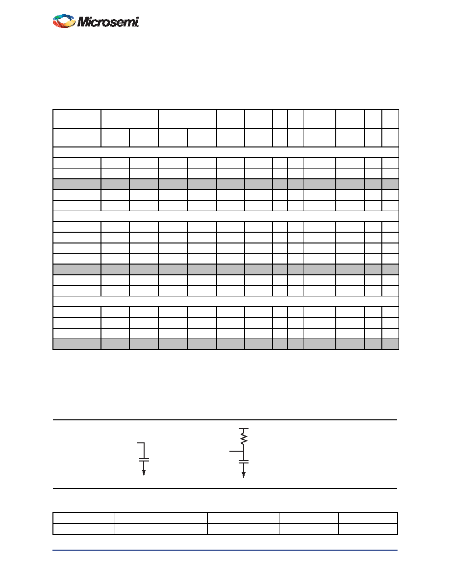
Table 2-102 Minimum and Maximum DC Input and Output Levels
3.3 V LVTTL /
3.3 V LVCMOS
VIL
VIH
VOL
VOH
IOL IOH
IOSL
IOSH
IIL1 IIH2
Drive Strength
Min.
V
Max.
V
Min.
V
Max.
V
Max.
V
Min.
VmA mA
Max.
mA3
Max.
mA3
A4 A4
Applicable to Pro I/O Banks
4 mA
–0.3
0.8
2
3.6
0.4
2.4
4
27
25
10
8 mA
–0.3
0.8
2
3.6
0.4
2.4
8
54
51
10
12 mA
–0.3
0.8
2
3.6
0.4
2.4
12
109
103
10
16 mA
–0.3
0.8
2
3.6
0.4
2.4
16
127
132
10
24 mA
–0.3
0.8
2
3.6
0.4
2.4
24
181
268
10
Applicable to Advanced I/O Banks
2 mA
–0.3
0.8
2
3.6
0.4
2.4
2
27
25
10
4 mA
–0.3
0.8
2
3.6
0.4
2.4
4
27
25
10
6 mA
–0.3
0.8
2
3.6
0.4
2.4
6
54
51
10
8 mA
–0.3
0.8
2
3.6
0.4
2.4
8
54
51
10
12 mA
–0.3
0.8
2
3.6
0.4
2.4
12
109
103
10
16 mA
–0.3
0.8
2
3.6
0.4
2.4
16
127
132
10
24 mA
–0.3
0.8
2
3.6
0.4
2.4
24
181
268
10
Applicable to Standard I/O Banks
2 mA
–0.3
0.8
2
3.6
0.4
2.4
2
27
25
10
4 mA
–0.3
0.8
2
3.6
0.4
2.4
4
27
25
10
6 mA
–0.3
0.8
2
3.6
0.4
2.4
6
54
51
10
8 mA
–0.3
0.8
2
3.6
0.4
2.4
8
54
51
10
Notes:
1. IIL is the input leakage current per I/O pin over recommended operation conditions where –0.3 V < VIN < VIL.
2. IIH is the input leakage current per I/O pin over recommended operating conditions VIH < VIN < VCCI. Input current is
larger when operating outside recommended ranges.
3. Currents are measured at high temperature (100°C junction temperature) and maximum voltage.
4. Currents are measured at 85°C junction temperature.
5. Software default selection highlighted in gray.
Figure 2-119 AC Loading
Table 2-103 AC Waveforms, Measuring Points, and Capacitive Loads
Input Low (V)
Input High (V)
Measuring Point* (V)
VREF (typ.) (V)
CLOAD (pF)
03.3
1.4
–
35
Note: *Measuring point = Vtrip. See Table 2-90 on page 2-169 for a complete table of trip points.
Test Point
Enable Path
Data Path
35 pF
R = 1 k
R to VCCI for tLZ / tZL / tZLS
R to GND for tHZ / tZH / tZHS
35 pF for tZH / tZHS / tZL / tZLS
35 pF for tHZ / tLZ
相關(guān)PDF資料 |
PDF描述 |
|---|---|
| AFS1500-2FG676I | IC FPGA 8MB FLASH 1.5M 676-FBGA |
| ASC49DREH-S734 | CONN EDGECARD 98POS .100 EYELET |
| M1AFS1500-2FGG676I | IC FPGA 8MB FLASH 1.5M 676-FBGA |
| RSC60DRTF-S13 | CONN EDGECARD 120POS .100 EXTEND |
| RMC60DRTF-S13 | CONN EDGECARD 120PS .100 EXTEND |
相關(guān)代理商/技術(shù)參數(shù) |
參數(shù)描述 |
|---|---|
| AFS1500-2PQ256ES | 制造商:ACTEL 制造商全稱(chēng):Actel Corporation 功能描述:Actel Fusion Mixed-Signal FPGAs |
| AFS1500-2PQ256I | 制造商:ACTEL 制造商全稱(chēng):Actel Corporation 功能描述:Actel Fusion Mixed-Signal FPGAs |
| AFS1500-2PQ256PP | 制造商:ACTEL 制造商全稱(chēng):Actel Corporation 功能描述:Actel Fusion Mixed-Signal FPGAs |
| AFS1500-2PQG256ES | 制造商:ACTEL 制造商全稱(chēng):Actel Corporation 功能描述:Actel Fusion Mixed-Signal FPGAs |
| AFS1500-2PQG256I | 制造商:ACTEL 制造商全稱(chēng):Actel Corporation 功能描述:Actel Fusion Mixed-Signal FPGAs |
發(fā)布緊急采購(gòu),3分鐘左右您將得到回復(fù)。