- 您現(xiàn)在的位置:買賣IC網(wǎng) > PDF目錄374045 > ADV7121KN50 (ANALOG DEVICES INC) CMOS 80 MHz, Triple 10-Bit Video DACs PDF資料下載
參數(shù)資料
| 型號: | ADV7121KN50 |
| 廠商: | ANALOG DEVICES INC |
| 元件分類: | DAC |
| 英文描述: | CMOS 80 MHz, Triple 10-Bit Video DACs |
| 中文描述: | TRIPLE, PARALLEL, 8 BITS INPUT LOADING, 10-BIT DAC, PDIP40 |
| 封裝: | 0.600 INCH, PLASTIC, DIP-40 |
| 文件頁數(shù): | 11/12頁 |
| 文件大小: | 196K |
| 代理商: | ADV7121KN50 |
ADV7121/ADV7122
–11–
REV. B
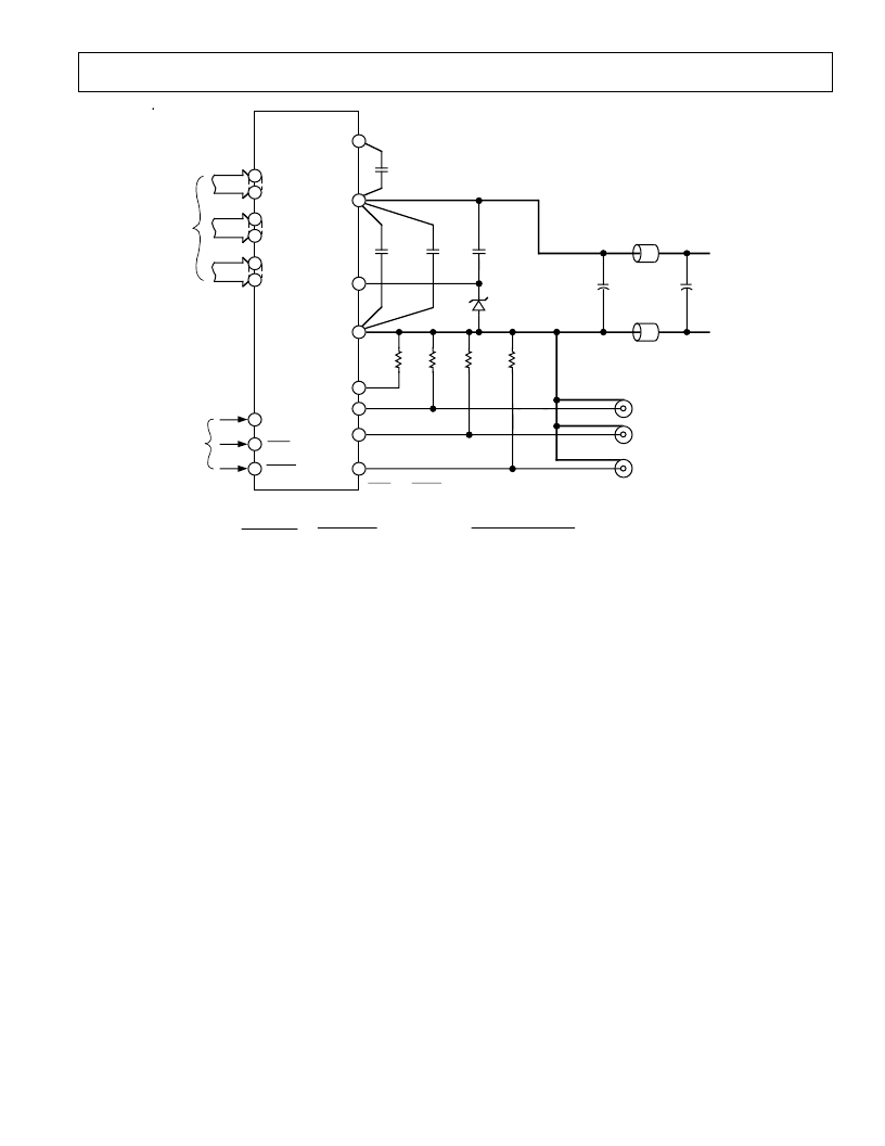
Supply Decoupling
Noise on the analog power plane can be further reduced by the
use of multiple decoupling capacitors (see Figure 8).
Optimum performance is achieved by the use of 0.1
μ
F ceramic
capacitors. Each of the two groups of V
AA
should be individually
decoupled to ground. T his should be done by placing the ca-
pacitors as close as possible to the device with the capacitor
leads as short as possible, thus minimizing lead inductance.
It is important to note that while the ADV7121/ADV7122 con-
tains circuitry to reject power supply noise, this rejection de-
creases with frequency. If a high frequency switching power
supply is used, the designer should pay close attention to reduce
ing power supply noise. A dc power supply filter (Murata
BNX 002) will provide EMI suppression between the switching
power supply and the main PCB. Alternatively, consideration
could be given to using a three terminal voltage regulator.
Digital Signal Interconnect
T he digital signal lines to the ADV7121/ADV7122 should be
isolated as much as possible from the analog outputs and other
analog circuitry. Digital signal lines should not overlay the ana-
log power plane.
Due to the high clock rates used, long clock lines to the
ADV7121/ADV7122 should be avoided so as to minimize noise
pickup.
Any active pull-up termination resistors for the digital inputs
should be connected to the regular PCB power plane (V
CC
),
and not the analog power plane.
Analog Signal Interconnect
T he ADV7121/ADV7122 should be located as close as possible
to the output connectors thus minimizing noise pickup and re-
flections due to impedance mismatch.
T he video output signals should overlay the ground plane, and
not the analog power plane, thereby maximizing the high fre-
quency power supply rejection.
For optimum performance, the analog outputs should each
have a source termination resistance to ground of 75
(doubly
terminated 75
configuration). T his termination resistance
should be as close as possible to the ADV7121/ADV7122 so as
to minimize reflections.
Additional information on PCB design is available in an appli-
cation note entitled “Design and Layout of a Video Graphics
System for Reduced EMI.” T his application note is available
from Analog Devices, publication no. E1309–15–10/89.
Figure 8. ADV7121/ADV7122 Typical Connection Diagram and Component List
GND
FS ADJUST
IOR
IOG
IOB
GROUND
ADV7121/ADV7122
C3
0.1
μ
F
C5
0.1
μ
F
Z1 (AD589)
R1
75
R2
75
R3
75
C1
33
μ
F
C2
10
μ
F
COMP
C6
0.1
μ
F
ANALOG POWER PLANE
L2 (FERRITE BEAD)
R0
R9
G0
G9
B0
B9
CLOCK
SYNC*
BLANK*
RGB
VIDEO
OUTPUT
VIDEO
DATA
INPUTS
VIDEO
CONTROL
INPUTS
ANALOG GROUND PLANE
C4
0.1
μ
F
L1 (FERRITE BEAD)
*SYNC and BLANK FUNCTIONS ARE NOT PROVIDED ON THE ADV7121.
V
AA
V
REF
+5V (V
CC
)
R
SET
560
COMPONENT
C1
C2
C3, C4, C5, C6
L1, L2
R1, R2, R3
R
SET
Z1
DESCRIPTION
33
μ
F TANTALUM CAPACITOR
10
μ
F TANTALUM
0.1
μ
F CERAMIC CAPACITOR
FERRITE BEAD
75
1% METAL FILM RESISTOR
560
1% METAL FILM RESISTOR
1.235V VOLTAGE REFERENCE
VENDOR PART NUMBER
FAIR-RITE 274300111 OR MURATA BL01/02/03
DALE CMF-55C
DALE CMF-55C
ANALOG DEVICES AD589JH
相關(guān)PDF資料 |
PDF描述 |
|---|---|
| ADV7121KN80 | CMOS 80 MHz, Triple 10-Bit Video DACs |
| ADV7122KST30 | CMOS 80 MHz, Triple 10-Bit Video DACs |
| ADV7122KST50 | CMOS 80 MHz, Triple 10-Bit Video DACs |
| ADV7121 | CMOS 80 MHz, Triple 10-Bit Video DACs |
| ADV7122KP30 | CMOS 80 MHz, Triple 10-Bit Video DACs |
相關(guān)代理商/技術(shù)參數(shù) |
參數(shù)描述 |
|---|---|
| ADV7121KN80 | 制造商:Rochester Electronics LLC 功能描述:- Bulk |
| ADV7122 | 制造商:AD 制造商全稱:Analog Devices 功能描述:CMOS 80 MHz, Triple 10-Bit Video DACs |
| ADV71226101 | 制造商:LG Corporation 功能描述:Frame Assembly |
| ADV7122JP30 | 制造商:未知廠家 制造商全稱:未知廠家 功能描述:Video DAC without Color Palette |
| ADV7122JP50 | 制造商:未知廠家 制造商全稱:未知廠家 功能描述:Video DAC without Color Palette |
發(fā)布緊急采購,3分鐘左右您將得到回復(fù)。