- 您現(xiàn)在的位置:買賣IC網(wǎng) > PDF目錄375264 > ADS7819UB 12-Bit 800kHz Sampling CMOS ANALOG-to-DIGITAL CONVERTER PDF資料下載
參數(shù)資料
| 型號(hào): | ADS7819UB |
| 英文描述: | 12-Bit 800kHz Sampling CMOS ANALOG-to-DIGITAL CONVERTER |
| 中文描述: | 12位800kHz采樣CMOS模擬數(shù)字轉(zhuǎn)換器 |
| 文件頁(yè)數(shù): | 3/11頁(yè) |
| 文件大小: | 317K |
| 代理商: | ADS7819UB |
2
ADS7819
3
SPECIFICATIONS
(CONT)
At T
A
= –40
°
C to +85
°
C, f
S
= 800kHz, +V
DIG
= +V
ANA
= +5V, –V
ANA
= –5V, using internal reference and the 50
input resistor shown in Figure 4b, unless otherwise specified.
ADS7819P, U
ADS7819PB, UB
PARAMETER
CONDITIONS
MIN
TYP
MAX
MIN
TYP
MAX
UNITS
POWER SUPPLIES
Specified Performance
+V
DIG
= +V
ANA
–V
ANA
+I
DIG
+I
ANA
–I
Derated Performance
+V
DIG
= +V
ANA
–V
ANA
Power Dissipation
+4.75
–5.25
+5
–5
+16
+16
–13
+5.25
–4.75
*
*
*
*
*
*
*
*
*
V
V
mA
mA
mA
+4.5
–5.5
+5
–5
225
+5.5
–4.5
275
*
*
*
*
*
*
*
V
V
f
S
= 800kHz
mW
TEMPERATURE RANGE
Specified Performance
Derated Performance
Storage
Thermal Resistance (
θ
JA
)
Plastic DIP
SOIC
–40
–55
–65
+85
+125
+150
*
*
*
*
*
*
°
C
°
C
°
C
75
75
*
*
°
C/W
°
C/W
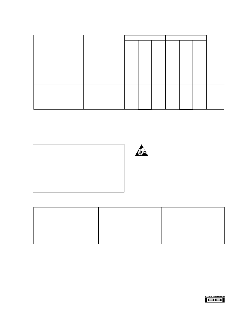
NOTES: (1) LSB means Least Significant Bit. For the 12-bit,
±
2.5V input ADS7819, one LSB is 1.22mV. (2) Typical rms noise at worst case transitions and
temperatures. (3) Measured with 50
in series with analog input. Adjustable to zero with external potentiometer. (4) Full scale error is the worst case of –Full Scale
or +Full Scale untrimmed deviation from ideal first and last code transitions, divided by the transition voltage (not divided by the full-scale range) and includes the
effect of offset error. (5) All specifications in dB are referred to a full-scale
±
2.5V input. (6) Usable Bandwidth defined as Full-Scale input frequency at which Signal-
to-(Noise+Distortion) degrades to 60dB, or 10 bits of accuracy. (7) Recovers to specified performance after 2 x FS input over voltage.
ABSOLUTE MAXIMUM RATINGS
Analog Inputs: V
..............................................................................
±
25V
REF .................................... +V
ANA
+0.3V to AGND2 –0.3V
CAP ...........................................Indefinite Short to AGND2
Momentary Short to +V
Ground Voltage Differences: DGND, AGND1, AGND2 ...................
±
0.3V
+V
ANA
...................................................................................................+7V
+V
DIG
to +V
.................................................................................+0.3V
+V
DIG
..................................................................................................... 7V
–V
................................................................................................... –7V
Digital Inputs ............................................................ –0.3V to +V
DIG
+0.3V
Maximum Junction Temperature ................................................... +165
°
C
Internal Power Dissipation ............................................................. 825mW
Lead Temperature (soldering, 10s)................................................ +300
°
C
MINIMUM
SIGNAL-TO-
(NOISE +
DISTORTION)
RATIO (dB)
MAXIMUM
INTEGRAL
LINEARITY
ERROR (LSB)
SPECIFICATION
TEMPERATURE
RANGE
PACKAGE DRAWING
NUMBER
(1)
MODEL
PACKAGE
ADS7819P
ADS7819PB
ADS7819U
ADS7819UB
±
1
68
70
68
70
–40
°
C to +85
°
C
–40
°
C to +85
°
C
–40
°
C to +85
°
C
–40
°
C to +85
°
C
28-Pin Plastic DIP
28-Pin Plastic DIP
28-Pin SOIC
28-Pin SOIC
246
246
217
217
±
0.75
±
1
±
0.75
ORDERING AND PACKAGE INFORMATION
NOTE: (1) For detailed drawing and dimension table, please see end of data sheet, or Appendix D of Burr-Brown IC Data Book.
ELECTROSTATIC
DISCHARGE SENSITIVITY
Electrostatic discharge can cause damage ranging from
performance degradation to complete device failure. Burr-
Brown Corporation recommends that all integrated circuits be
handled and stored using appropriate ESD protection
methods.
相關(guān)PDF資料 |
PDF描述 |
|---|---|
| ADS7819 | CMOS Dual 4-Input NOR Gate 14-SOIC -55 to 125 |
| ADS7819P | CMOS Dual 4-Input NOR Gate 14-SOIC -55 to 125 |
| ADS7819U | 12-Bit 800kHz Sampling CMOS ANALOG-to-DIGITAL CONVERTER |
| ADS7820 | CMOS Dual 4-Input NOR Gate 14-SOIC -55 to 125 |
| ADS7820P | 12-Bit 10ms Sampling CMOS ANALOG-to-DIGITAL CONVERTER |
相關(guān)代理商/技術(shù)參數(shù) |
參數(shù)描述 |
|---|---|
| ADS7820 | 制造商:BB 制造商全稱:BB 功能描述:12-Bit 10ms Sampling CMOS ANALOG-to-DIGITAL CONVERTER |
| ADS7820P | 制造商:Rochester Electronics LLC 功能描述:- Bulk 制造商:BURR BROWN 功能描述:ANALOG 2000 DC S8J2B 制造商:Texas Instruments 功能描述: |
| ADS7820PB | 功能描述:模數(shù)轉(zhuǎn)換器 - ADC 12bit 10 Micro-Sec RoHS:否 制造商:Texas Instruments 通道數(shù)量:2 結(jié)構(gòu):Sigma-Delta 轉(zhuǎn)換速率:125 SPs to 8 KSPs 分辨率:24 bit 輸入類型:Differential 信噪比:107 dB 接口類型:SPI 工作電源電壓:1.7 V to 3.6 V, 2.7 V to 5.25 V 最大工作溫度:+ 85 C 安裝風(fēng)格:SMD/SMT 封裝 / 箱體:VQFN-32 |
| ADS7820U | 制造商:Rochester Electronics LLC 功能描述:- Bulk |
| ADS7820UB | 制造商:Rochester Electronics LLC 功能描述:- Bulk |
發(fā)布緊急采購(gòu),3分鐘左右您將得到回復(fù)。