- 您現(xiàn)在的位置:買賣IC網(wǎng) > PDF目錄375264 > ADS7817 12-Bit Differential Input Micro Power Sampling ANALOG-TO-DIGITAL CONVERTER PDF資料下載
參數(shù)資料
| 型號(hào): | ADS7817 |
| 英文描述: | 12-Bit Differential Input Micro Power Sampling ANALOG-TO-DIGITAL CONVERTER |
| 中文描述: | 12位差分輸入微功耗采樣模擬到數(shù)字轉(zhuǎn)換器 |
| 文件頁數(shù): | 8/15頁 |
| 文件大小: | 172K |
| 代理商: | ADS7817 |
8
ADS7817
THEORY OF OPERATION
The ADS7817 is a classic successive approximation register
(SAR) analog-to-digital (A/D) converter. The architecture is
based on capacitive redistribution which inherently includes
a sample/hold function. The converter is fabricated on a 0.6
μ
CMOS process. The architecture and process allow the
ADS7817 to acquire and convert an analog signal at up to
200,000 conversions per second while consuming very little
power.
The ADS7817 requires an external reference, an external
clock, and a single +5V power source. The external refer-
ence can be any voltage between 100mV and 2.5V. The
value of the reference voltage directly sets the range of the
analog input. The reference input current depends on the
conversion rate of the ADS7817.
The external clock can vary between 10kHz (625Hz through-
put) and 3.2MHz (200kHz throughput). The duty cycle of
the clock is essentially unimportant as long as the minimum
high and low times are at least 150ns. The minimum clock
frequency is set by the leakage on the capacitors internal to
the ADS7817.
The analog input is provided to two input pins: +In and –In.
When a conversion is initiated, the differential input on these
pins is sampled on the internal capacitor array. While a
conversion is in progress, both inputs are disconnected from
any internal function.
The digital result of the conversion is clocked out by the
DCLOCK input and is provided serially, most significant bit
first, on the D
OUT
pin. The digital data that is provided on the
D
OUT
pin is for the conversion currently in progress—there
is no pipeline delay. It is possible to continue to clock the
ADS7817 after the conversion is complete and to obtain the
serial data least significant bit first. See the Digital Interface
section for more information.
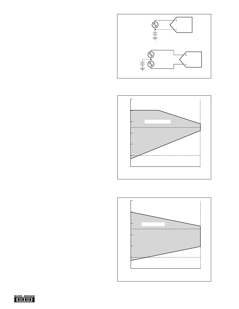
ANALOG INPUT
The analog input is bipolar and fully differential. There are
two general methods of driving the analog input of the
ADS7817: single-ended or differential (see Figure 1). When
the input is single-ended, the –In input is held at a fixed
voltage. The +In input swings around the same voltage and
the peak-to-peak amplitude is 2 V
REF
. The value of V
REF
determines the range over which the common voltage may
vary (see Figure 2).
When the input is differential, the amplitude of the input is the
difference between the +In and –In input, or: +In – (–In). A
voltage or signal is common to both of these inputs. The peak-
to-peak amplitude of each input is V
REF
about this common
voltage. However, since the inputs are 180
°
out of phase, the
peak-to-peak amplitude of the difference voltage is 2 V
REF
.
The value of V
REF
also determines the range of the voltage
that may be common to both inputs (see Figure 3).
FIGURE 1. Methods of Driving the ADS7817: Single-
Ended or Differential.
FIGURE 2. Single-Ended Input: Common Voltage Range vs
V
REF
.
FIGURE 3. Differential Input: Common Voltage Range vs
V
REF
.
ADS7817
ADS7817
Single-Ended Input
Common
Voltage
2 V
peak-to-peak
Differential Input
Common
Voltage
V
peak-to-peak
V
peak-to-peak
0.0
0.5
1.0
1.5
2.0
2.5
V
REF
(V)
C
–1
0
1
2
3
4
5
2.8
2.2
–0.3
4.0
V
CC
= 5V
Single-Ended Input
0.0
0.5
1.0
1.5
2.0
2.5
V
REF
(V)
2.75
V
CC
= 5V
1.95
4.0
–0.3
C
–1
0
1
2
3
4
5
Differential Input
相關(guān)PDF資料 |
PDF描述 |
|---|---|
| ADS7817B | 12-Bit Differential Input Micro Power Sampling ANALOG-TO-DIGITAL CONVERTER |
| ADS7817C | 12-Bit Differential Input Micro Power Sampling ANALOG-TO-DIGITAL CONVERTER |
| ADS7818 | 2SC5161 |
| ADS7818E | 2SC5161 |
| ADS7818EB | 2SC5161 |
相關(guān)代理商/技術(shù)參數(shù) |
參數(shù)描述 |
|---|---|
| ADS7817B | 制造商:BB 制造商全稱:BB 功能描述:12-Bit Differential Input Micro Power Sampling ANALOG-TO-DIGITAL CONVERTER |
| ADS7817C | 制造商:BB 制造商全稱:BB 功能描述:12-Bit Differential Input Micro Power Sampling ANALOG-TO-DIGITAL CONVERTER |
| ADS7817E | 制造商:TI 制造商全稱:Texas Instruments 功能描述:12-Bit Differential Input Micro Power Sampling |
| ADS7817E/250 | 功能描述:模數(shù)轉(zhuǎn)換器 - ADC 12-Bit Differential In MicroPwr Sampling RoHS:否 制造商:Texas Instruments 通道數(shù)量:2 結(jié)構(gòu):Sigma-Delta 轉(zhuǎn)換速率:125 SPs to 8 KSPs 分辨率:24 bit 輸入類型:Differential 信噪比:107 dB 接口類型:SPI 工作電源電壓:1.7 V to 3.6 V, 2.7 V to 5.25 V 最大工作溫度:+ 85 C 安裝風(fēng)格:SMD/SMT 封裝 / 箱體:VQFN-32 |
| ADS7817E/250G4 | 功能描述:模數(shù)轉(zhuǎn)換器 - ADC 12-Bit Differential In MicroPwr Sampling RoHS:否 制造商:Texas Instruments 通道數(shù)量:2 結(jié)構(gòu):Sigma-Delta 轉(zhuǎn)換速率:125 SPs to 8 KSPs 分辨率:24 bit 輸入類型:Differential 信噪比:107 dB 接口類型:SPI 工作電源電壓:1.7 V to 3.6 V, 2.7 V to 5.25 V 最大工作溫度:+ 85 C 安裝風(fēng)格:SMD/SMT 封裝 / 箱體:VQFN-32 |
發(fā)布緊急采購,3分鐘左右您將得到回復(fù)。