- 您現(xiàn)在的位置:買賣IC網(wǎng) > PDF目錄375263 > ADS1252U 24-Bit, 40kHz ANALOG-TO-DIGITAL CONVERTER PDF資料下載
參數(shù)資料
| 型號: | ADS1252U |
| 英文描述: | 24-Bit, 40kHz ANALOG-TO-DIGITAL CONVERTER |
| 中文描述: | 24位40kHz的模擬到數(shù)字轉(zhuǎn)換器 |
| 文件頁數(shù): | 7/14頁 |
| 文件大小: | 131K |
| 代理商: | ADS1252U |
7
ADS1252
REFERENCE INPUT
Reference input takes an average current of 220
μ
A with a
16MHz system clock. This current will be proportional to
the system clock. A buffered reference is needed for
ADS1252. The recommended reference circuit is shown in
Figure 2.
Reference voltages higher than 4.096V will increase the
full-scale range, while the absolute internal circuit noise of
the converter remains the same. This will decrease the noise
in terms of ppm of full scale, which increases the effective
resolution.
Reference voltages lower than 4.096V will decrease the full-
scale range, while the absolute internal circuit noise at the
converter remains the same. This will increase the noise in
terms of ppm of full scale. Therefore, the use of a lower
reference voltage will reduce the effective resolution.
DIGITAL FILTER
The digital filter of the ADS1252, referred to as a sinc
5
filter,
computes the digital result based on the most recent outputs
from the delta-sigma modulator. At the most basic level, the
digital filter can be thought of as simply averaging the
modulator results in a weighted form and presenting this
average as the digital output. The digital output rate, or data
rate, scales directly with the system CLK frequency. This
allows the data output rate to be changed over a very wide
range (five orders of magnitude) by changing the system
CLK frequency. However, it is important to note that the
–3dB point of the filter is 0.216 times the data output rate,
so the data output rate should allow for sufficient margin to
prevent attenuation of the signal of interest.
Since the conversion result is essentially an average, the data
output rate determines the location of the resulting notches
in the digital filter (see Figure 3). Note that the first notch is
located at the data output rate frequency, and subsequent
notches are located at integer multiples of the data output
rate to allow for rejection of not only the fundamental
frequency, but also harmonic frequencies. In this manner,
the data output rate can be used to set specific notch
frequencies in the digital filter response. For example, if the
rejection of power line frequencies is desired, then the data
output rate can simply be set to the power line frequency.
For 50Hz rejection, the system CLK frequency should be
19.200kHz, this will set the data output rate to 50Hz (see
Table I and Figure 4). For 60Hz rejection, the system CLK
frequency should be 20.040kHz, this will set the data output
rate to 60Hz (see Table I and Figure 5). If both 50Hz and
60Hz rejection is required, then the system CLK should be
3.840kHz; this will set the data output rate to 10Hz and
reject both 50Hz and 60Hz (See Table I and Figure 6).
There is an additional benefit in using a lower data output
rate. It provides better rejection of signals in the frequency
band of interest. For example, with a 50Hz data output rate,
a significant signal at 75Hz may alias back into the passband
at 25Hz. This is due to the fact that rejection at 75Hz may
only be 66dB in the stopband—frequencies higher than the
first notch frequency (see Figure 4). However, setting the
data output rate to 10Hz will provide 135 dB rejection at
75Hz (see Figure 6). A similar benefit is gained at frequen-
cies near the data output rate (see Figures 7, 8, 9, and 10).
For example, with a 50Hz data output rate, rejection at 55Hz
may only be 105dB (see Figure 7). However, with a 10Hz
data output rate, rejection at 55Hz will be 122dB (see Figure
8). If a slower data output rate does not meet the system
requirements, then the analog front end can be designed to
provide the needed attenuation to prevent aliasing. Addition-
ally the data output rate may be increased and additional
digital filtering may be done in the processor or controller.
The digital filter is described by the following transfer
function:
H( )
f
f
f
f
or
H( )
z
z
MOD
MOD
sin
sin
–
(
–
–
–
=
=
)
π
π
64
64
1
64
1
5
64
1
5
0.10
μ
F
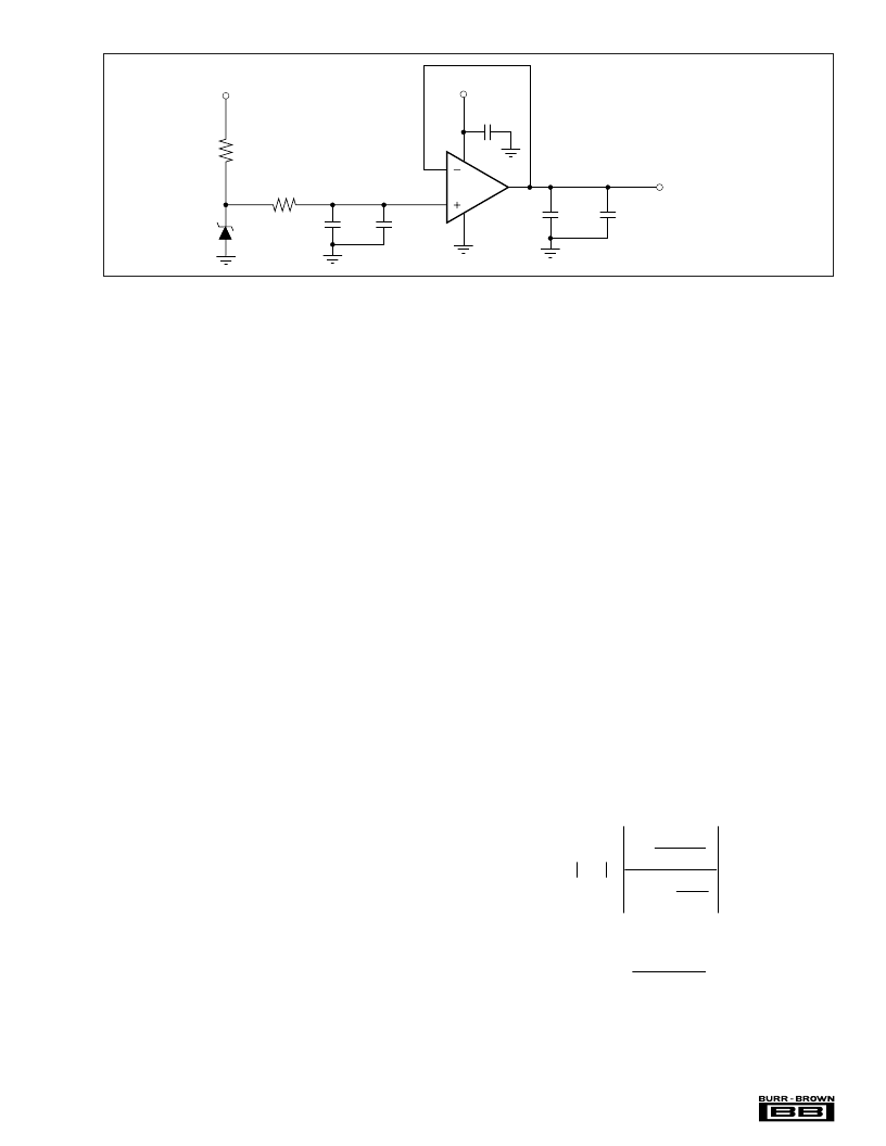
+5V
+5V
4.99k
10k
10
μ
F
LM404-4.1
4
3
1
2
7
6
+
0.10
μ
F
0.1
μ
F
10
μ
F
+
OPA350
To V
Pin 8 of
the ADS1252
FIGURE 2. Recommended External Voltage Reference Circuit for Best Low Noise Operation with the ADS1252.
The digital filter requires five conversions to fully settle. The
modulator has an oversampling ratio of 64, therefore, it
requires 5 64, or 320 modulator results, or clocks, to fully
settle. Since the modulator clock is derived from the system
相關(guān)PDF資料 |
PDF描述 |
|---|---|
| ADS1252K5 | 24-Bit, 20kHz, Low-Power ANALOG-TO-DIGITAL CONVERTER |
| ADS1254 | 24-Bit, 20kHz, Low Power ANALOG-TO-DIGITAL CONVERTER |
| ADS1254E | 24-Bit, 20kHz, Low Power ANALOG-TO-DIGITAL CONVERTER |
| ADS1255IDB | Very Low Noise, 24-Bit Analog-to-Digital Converter |
| ADS1255IDBR | Very Low Noise, 24-Bit Analog-to-Digital Converter |
相關(guān)代理商/技術(shù)參數(shù) |
參數(shù)描述 |
|---|---|
| ADS1252U | 制造商:Texas Instruments 功能描述:IC 24BIT ADC 41.7KSPS SMD |
| ADS1252U/2K5 | 功能描述:模數(shù)轉(zhuǎn)換器 - ADC ResolutionPlus 24-Bit 40kHz RoHS:否 制造商:Texas Instruments 通道數(shù)量:2 結(jié)構(gòu):Sigma-Delta 轉(zhuǎn)換速率:125 SPs to 8 KSPs 分辨率:24 bit 輸入類型:Differential 信噪比:107 dB 接口類型:SPI 工作電源電壓:1.7 V to 3.6 V, 2.7 V to 5.25 V 最大工作溫度:+ 85 C 安裝風(fēng)格:SMD/SMT 封裝 / 箱體:VQFN-32 |
| ADS1252U/2K5G4 | 功能描述:模數(shù)轉(zhuǎn)換器 - ADC ResolutionPlus 24-Bit 40kHz RoHS:否 制造商:Texas Instruments 通道數(shù)量:2 結(jié)構(gòu):Sigma-Delta 轉(zhuǎn)換速率:125 SPs to 8 KSPs 分辨率:24 bit 輸入類型:Differential 信噪比:107 dB 接口類型:SPI 工作電源電壓:1.7 V to 3.6 V, 2.7 V to 5.25 V 最大工作溫度:+ 85 C 安裝風(fēng)格:SMD/SMT 封裝 / 箱體:VQFN-32 |
| ADS1252UG4 | 功能描述:模數(shù)轉(zhuǎn)換器 - ADC ResolutionPlus 24-Bit 40kHz RoHS:否 制造商:Texas Instruments 通道數(shù)量:2 結(jié)構(gòu):Sigma-Delta 轉(zhuǎn)換速率:125 SPs to 8 KSPs 分辨率:24 bit 輸入類型:Differential 信噪比:107 dB 接口類型:SPI 工作電源電壓:1.7 V to 3.6 V, 2.7 V to 5.25 V 最大工作溫度:+ 85 C 安裝風(fēng)格:SMD/SMT 封裝 / 箱體:VQFN-32 |
| ADS1253 | 制造商:TI 制造商全稱:Texas Instruments 功能描述:24-Bit, 20kHz, Low Power ANALOG-TO-DIGITAL CONVERTER |
發(fā)布緊急采購,3分鐘左右您將得到回復(fù)。