- 您現(xiàn)在的位置:買(mǎi)賣(mài)IC網(wǎng) > PDF目錄374023 > ADP3810AR-12.6 (ANALOG DEVICES INC) IC-OFF-LINE BATT.CHARGER PDF資料下載
參數(shù)資料
| 型號(hào): | ADP3810AR-12.6 |
| 廠(chǎng)商: | ANALOG DEVICES INC |
| 元件分類(lèi): | 電源管理 |
| 英文描述: | IC-OFF-LINE BATT.CHARGER |
| 中文描述: | 1-CHANNEL POWER SUPPLY SUPPORT CKT, PDSO8 |
| 封裝: | SOIC-8 |
| 文件頁(yè)數(shù): | 10/16頁(yè) |
| 文件大小: | 457K |
| 代理商: | ADP3810AR-12.6 |
第1頁(yè)第2頁(yè)第3頁(yè)第4頁(yè)第5頁(yè)第6頁(yè)第7頁(yè)第8頁(yè)第9頁(yè)當(dāng)前第10頁(yè)第11頁(yè)第12頁(yè)第13頁(yè)第14頁(yè)第15頁(yè)第16頁(yè)
ADP3810/ADP3811
–10–
REV. 0
battery voltage is at least 1.5 V with a programmed charge cur-
rent of 0.1 A. For a higher programmed charge current, the
battery voltage can drop below 1.5 V, and V
CC
is still maintained
above 2.7 V. This is because of the additional energy in the
flyback transformer, which transfers more energy through the
10 nF capacitor to V
CC
. The 22
μ
F bypass capacitor on V
CC
stores the energy transferred through the 10 nF capacitor.
Secondary Side Component Calculations
Design Criteria:
Charging a 6 cell NiCad battery.
Max Individual Cell Voltage:
Max Battery Stack Voltage:
Max Charge Current:
Max Control Voltage:
R
S
Fixed Value:
Pick a Value for R1:
The voltage limit of 10 V is approximately 10% above the maxi-
mum fully charged voltage when –
V/
t termination is used.
This limit gives a second level of protection without interfering
with –
V/
t charge termination.
Component Value Calculations:
Current Sense Resistor:
R
CS
= V
CTRL
/(4
×
I
OMAX
) = 1/(4
×
1)
= 0.25 W, 1%, 0.5 W
Battery Divider, R2:
R2 = V
REF
×
R1/(V
OMAX
–V
REF
)
R2 = 2
80.6 k
/(10 V–2 V) =
20.15 k
, Pick 20.0 k
The final voltage and charge current accuracy is dependent
upon the resistor tolerances. Choose appropriate tolerances for
the desired accuracy. One percent accuracy is recommended.
V
CELLMAX
= 1.67 V
V
OMAX
= 6
×
1.67 V = 10 V
I
OMAX
= 1 A
V
CTRL
= 1 V (for I
OMAX
= 1 A)
R
S
= 20 k
R1 = 80.6 k
Charger Performance Summary
The charger circuit properly executes the charging algorithm ex-
hibiting stable operation regardless of battery conditions, includ-
ing an open circuit load. The circuit can charge to other battery
voltages by modifying only the battery voltage sense divider. As
would be expected, circuit efficiency is best at high battery volt-
ages. Replacing the output blocking rectifier diode with a
Schottky would improve efficiency if the Schottky’s leakage
could be tolerated, and its reverse voltage rating met the appli-
cation requirement.
V
OUT
1.0
0.3
0.0
2
11
3
I
L
4
5
6
7
8
9
10
0.9
0.4
0.2
0.1
0.8
0.6
0.7
0.5
V
CTRL
= 0.125V
V
CTRL
= 0.25V
V
CTRL
= 0.5V
V
CTRL
= 1.0V
Figure 24. Charge Current vs. Battery Voltage at Four Set-
tings for the Flyback Charger in Figure 23
The Battery Charge Current vs. Battery Voltage characteristics
for four different charge current settings are given in Figure 24.
The high gain of the internal amplifiers ensures the sharp transi-
tion between current mode and voltage mode regardless of the
charge current setting. The fact that the current remains at full
charging until the battery is very close to its final voltage ensures
fast charging times.
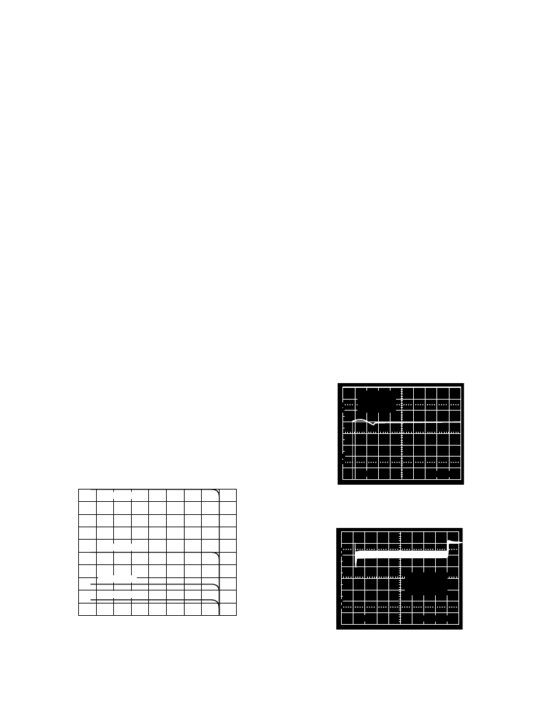
The transient performance for various turn-on and turn-off con-
ditions is detailed in Figures 25, 26 and 27. Figure 25 shows
the output voltage when power is applied with no battery con-
nected. As shown, the output voltage quickly rises and over-
shoots its set voltage. The internal comparator responds to this
and clamps the voltage giving a quick recovery. Without the in-
ternal comparator, an external zener would be required to clamp
the voltage to the LED anode. Figure 26 shows the battery cur-
rent when connecting and disconnecting a battery. The actual
trace shown is the voltage across R
CS
, which is negative for cur-
rent flowing into the battery. There is an overshoot when the
battery is connected, but the loop quickly takes control and lim-
its the average current to the programmed 0.75 A. When the
battery is removed, the current quickly returns to zero. The
solid band on the scope is due to the current rising and falling
with the switching of the PWM. The time scale is too slow to
show the detail of this. Figure 27 shows the output voltage
when a battery stack charged to 6 V is connected and then dis-
connected. As expected, when the battery is connected, the
voltage immediately goes to 6 V. When the battery is discon-
nected, the voltage returns to the programmed float voltage of
10 V. Again, a small overshoot is present that is clamped by the
internal comparator.
10
0%
100
90
0.1sec/DIV
2V/DIV
T
A
= +25
8
C
NO BATTERY
V
IN
= 220V
AC
10V
0V
Figure 25. Flyback Charger Output Voltage Transient at
Power Turn On, No Battery Attached
10
0%
100
90
20msec/DIV
0.2V/DIV
0.0V
–200mV
T
A
= +25
8
C
V
CTRL
= 0.775V
V
IN
= 220V
AC
Figure 26. Charge Current Transient Response to Battery
Connect/Disconnect
相關(guān)PDF資料 |
PDF描述 |
|---|---|
| ADP3810AR-84 | Secondary Side, Off-Line Battery Charger Controllers |
| ADP3811AR | Secondary Side, Off-Line Battery Charger Controllers |
| ADP3810AR-126 | Top Entry Connector Hood; Enclosure Material:Aluminum Alloy; For Use With:C146 Rectangular Circular Connectors; Connecting Termination:Screw; Gender:Male; No. of Contacts:48; Operating Voltage:400V; Series:C-146 RoHS Compliant: Yes |
| ADP3810AR-168 | Circular Connector Cable Assembly; Connector Type A:Circular Plug; Connector Type B:Stripped End Leads; Cable Length:10ft; Features:500 Mating Cycles, PVC Jacket, IP67 Rating, E63093 Rated Connector; No. of Contacts:3 RoHS Compliant: Yes |
| ADP3820AR-41 | Circular Connector Cable Assembly; Connector Type A:Circular Receptacle; Connector Type B:Stripped End Leads; Cable Length:10ft RoHS Compliant: Yes |
相關(guān)代理商/技術(shù)參數(shù) |
參數(shù)描述 |
|---|---|
| ADP3810AR-16.8 | 制造商:Analog Devices 功能描述:Battery Charger 6mA 16.8V 8-Pin SOIC N 制造商:Rochester Electronics LLC 功能描述:- Bulk |
| ADP3810AR-168 | 制造商:AD 制造商全稱(chēng):Analog Devices 功能描述:Secondary Side, Off-Line Battery Charger Controllers |
| ADP3810AR-4.2 | 制造商:Rochester Electronics LLC 功能描述:OFF-LINE BATTERY CHARGER CONTROLLER-4.2V - Bulk 制造商:Analog Devices 功能描述: |
| ADP3810AR-42 | 制造商:AD 制造商全稱(chēng):Analog Devices 功能描述:Secondary Side, Off-Line Battery Charger Controllers |
| ADP3810AR-8.4 | 制造商:Analog Devices 功能描述:Battery Charger 6mA 8.4V 8-Pin SOIC N 制造商:Rochester Electronics LLC 功能描述:- Bulk |
發(fā)布緊急采購(gòu),3分鐘左右您將得到回復(fù)。