- 您現(xiàn)在的位置:買賣IC網(wǎng) > PDF目錄374018 > ADP1108AR-12 (ANALOG DEVICES INC) Circular Connector; No. of Contacts:128; Series:LJT06R; Body Material:Aluminum; Connecting Termination:Crimp; Connector Shell Size:25; Circular Contact Gender:Pin; Circular Shell Style:Straight Plug; Insert Arrangement:25-35 PDF資料下載
參數(shù)資料
| 型號: | ADP1108AR-12 |
| 廠商: | ANALOG DEVICES INC |
| 元件分類: | 穩(wěn)壓器 |
| 英文描述: | Circular Connector; No. of Contacts:128; Series:LJT06R; Body Material:Aluminum; Connecting Termination:Crimp; Connector Shell Size:25; Circular Contact Gender:Pin; Circular Shell Style:Straight Plug; Insert Arrangement:25-35 |
| 中文描述: | 1.5 A SWITCHING REGULATOR, 25 kHz SWITCHING FREQ-MAX, PDSO8 |
| 封裝: | SOIC-8 |
| 文件頁數(shù): | 8/12頁 |
| 文件大?。?/td> | 234K |
| 代理商: | ADP1108AR-12 |
ADP1108
–8–
REV. 0
10
0%
5
m
s
50mV
100
90
C
OUT
=100
m
F, 16V
I
SW
= 500mA
ESR
z
0.18
V
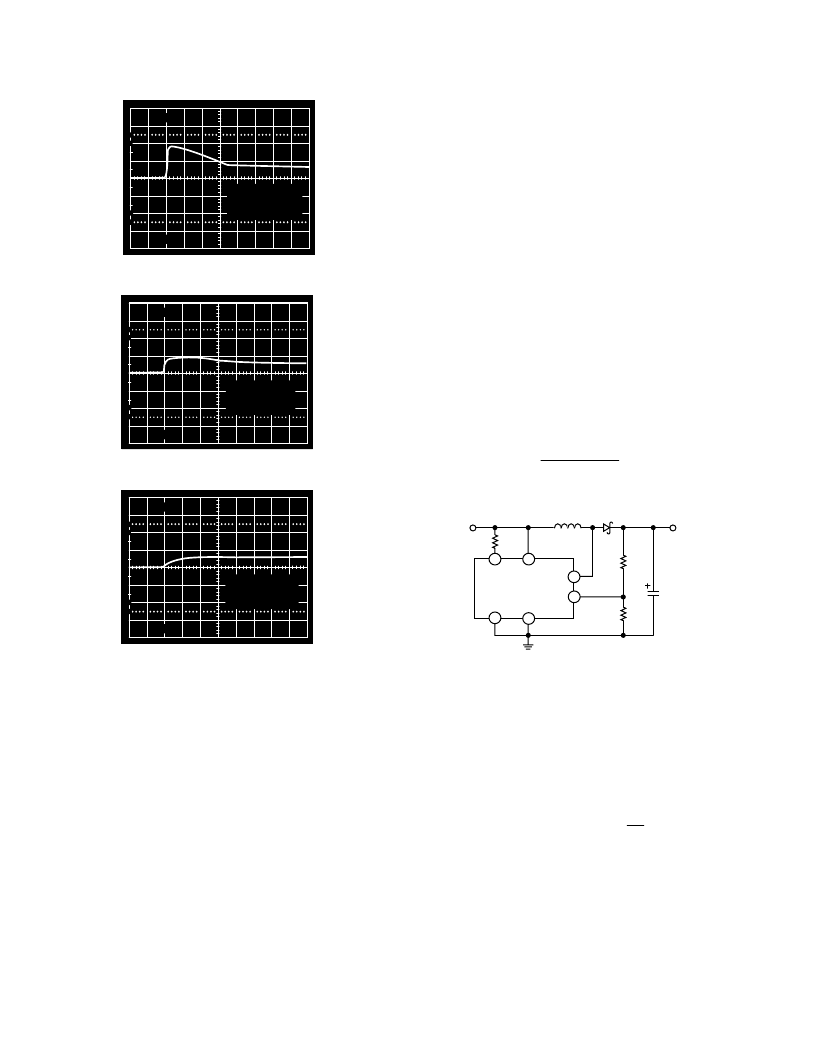
Figure 12. Aluminum Electrolytic
10
0%
5μs
50mV
100
90
C
OUT
=100μF, 6V
I
SW
= 500mA
ESR
z
0.07
V
Figure 13. Tantalum Electrolytic
10
0%
5
m
s
50mV
100
90
C
OUT
=100
m
F, 16V
I
SW
= 500mA
ESR
z
0.02
V
Figure 14. OS-CON Capacitor
If low output ripple is important, the user should consider using
the ADP3000. T his device switches at 400 kHz, which simpli-
fies the design of the output filter. Consult the ADP3000 data
sheet for additional details.
DIODE SE LE CT ION
In specifying a diode, consideration must be given to speed, for-
ward voltage drop and reverse leakage current. When the
ADP1108 switch turns off, the diode must turn on rapidly if
high efficiency is to be maintained. Schottky rectifiers, as well as
fast signal diodes such as the 1N4148, are appropriate. T he for-
ward voltage of the diode represents power that is not delivered
to the load, so V
F
must also be minimized. Again, Schottky di-
odes are recommended. Leakage current is especially important
in low-current applications, where the leakage can be a signifi-
cant percentage of the total quiescent current.
For most circuits, the 1N5818 is a suitable companion to the
ADP1108. T his diode has a V
F
of 0.5 V at 1 A, 4
μ
A to 10
μ
A
leakage and fast turn-on and turn-off times. A surface mount
version, the MBRS130T 3, is also available.
For switch currents of 100 mA or less, a Schottky diode such
as the BAT 85 provides a V
F
of 0.8 V at 100 mA and leakage
less than 1
μ
A. A similar device, the BAT 54, is available in an
SOT -23 package. Even lower leakage, in the 1 nA to 5 nA
range, can be obtained with a 1N4148 signal diode.
General purpose rectifiers, such as the 1N4001, are not suitable for
ADP1108 circuits. T hese devices, which have turn-on times of
10
μ
s or more, are far too slow for switching power supply applica-
tions. Using such a diode “just to get started” will result in wasted
time and effort. Even if an ADP1108 circuit appears to function
with a 1N4001, the resulting performance will not be indicative of
the circuit performance when the correct diode is used.
Circuit Operation, Step-Up (Boost) Mode
In boost mode, the ADP1108 produces an output voltage higher
than the input voltage. For example, +12 V can be generated
from a +5 V logic power supply or +5 V can be derived from
two alkaline cells (+3 V).
Figure 15 shows an ADP1108 configured for step-up operation.
T he collector of the internal power switch is connected to the out-
put side of the inductor, while the emitter is connected to GND.
When the switch turns on, Pin SW1 is pulled near ground. T his ac-
tion forces a voltage across L1 equal to V
IN
2
V
CE(SAT )
, and current
begins to flow through L 1. T his current reaches a final value
(ignoring second-order effects) of:
I
PEAK
V
IN
±
V
CE
(
SAT
)
L
×
36
μ
s
where 36
μ
s is the ADP1108 switch’s “on” time.
3
5
1
8
4
2
I
LIM
V
IN
SW1
FB
SW2
GND
ADP1108
L1
D1
V
OUT
C1
R3
R1
R2
V
IN
Figure 15. Step-Up Mode Operation
When the switch turns off, the magnetic field collapses. T he
polarity across the inductor changes, current begins to flow
through D1 into the load and the output voltage is driven above
the input voltage.
T he output voltage is fed back to the ADP1108 via resistors R1
and R2. When the voltage at Pin FB falls below 1.245 V, SW1
turns “on” again and the cycle repeats. T he output voltage is
therefore set by the formula:
V
OUT
=
1.245
V
×
1
+
R
1
R
2
T he circuit of Figure 15 shows a direct current path from V
IN
to
V
OUT
, via the inductor and D1. T herefore, the boost converter
is not protected if the output is short circuited to ground.
Circuit Operation, Step-Down (Buck) Mode
T he ADP1108’s step-down mode is used to produce an output
voltage lower than the input voltage. For example, the output of
four NiCd cells (+4.8 V) can be converted to a +3 V logic supply.
A typical configuration for step-down operation of the ADP1108 is
shown in Figure 16. In this case, the collector of the internal power
switch is connected to V
IN
and the emitter drives the inductor.
相關(guān)PDF資料 |
PDF描述 |
|---|---|
| ADP1108AR-33 | Circular Connector; No. of Contacts:128; Series:LJT06R; Body Material:Aluminum; Connecting Termination:Crimp; Connector Shell Size:25; Circular Contact Gender:Pin; Circular Shell Style:Straight Plug; Insert Arrangement:25-35 |
| ADP1108AR-5 | Circular Connector; No. of Contacts:128; Series:LJT06R; Body Material:Aluminum; Connecting Termination:Crimp; Connector Shell Size:25; Circular Contact Gender:Pin; Circular Shell Style:Straight Plug; Insert Arrangement:25-35 |
| ADP1109AAN-12 | Circular Connector; MIL SPEC:MIL-C-5015; Body Material:Metal; Series:GT; No. of Contacts:7; Connector Shell Size:16S; Connecting Termination:Solder; Circular Shell Style:Square Flange Receptacle; Body Style:Straight |
| ADP1109AAN-33 | Micropower Low Cost Fixed 3.3 V, 5 V, 12 V and Adjustable DC-to-DC Converter |
| ADP1109AAN-5 | Micropower Low Cost Fixed 3.3 V, 5 V, 12 V and Adjustable DC-to-DC Converter |
相關(guān)代理商/技術(shù)參數(shù) |
參數(shù)描述 |
|---|---|
| ADP1108AR-3.3 | 制造商:Rochester Electronics LLC 功能描述:MICROPOWER DC-DC CONVERTER 3.3V - Bulk |
| ADP1108AR-33 | 制造商:AD 制造商全稱:Analog Devices 功能描述:Micropower DC-DC Converter Adjustable and Fixed 3.3 V, 5 V, 12 V |
| ADP1108AR-5 | 制造商:Rochester Electronics LLC 功能描述:- Bulk |
| ADP1109 | 制造商:AD 制造商全稱:Analog Devices 功能描述:Micropower Low Cost Fixed 3.3 V, 5 V, 12 V and Adjustable DC-to-DC Converter |
| ADP1109A | 制造商:AD 制造商全稱:Analog Devices 功能描述:Micropower Low Cost Fixed 3.3 V, 5 V, 12 V and Adjustable DC-to-DC Converter |
發(fā)布緊急采購,3分鐘左右您將得到回復(fù)。