- 您現(xiàn)在的位置:買賣IC網(wǎng) > PDF目錄97842 > ADL5380ACPZ-WP (ANALOG DEVICES INC) 400 MHz - 6000 MHz RF/MICROWAVE I/Q DEMODULATOR PDF資料下載
參數(shù)資料
| 型號: | ADL5380ACPZ-WP |
| 廠商: | ANALOG DEVICES INC |
| 元件分類: | 調(diào)制器/解調(diào)器 |
| 英文描述: | 400 MHz - 6000 MHz RF/MICROWAVE I/Q DEMODULATOR |
| 封裝: | 4 X 4 MM, ROHS COMPLIANT, MO-220-VGGD-8, LFCSP-24 |
| 文件頁數(shù): | 19/36頁 |
| 文件大小: | 833K |
| 代理商: | ADL5380ACPZ-WP |
第1頁第2頁第3頁第4頁第5頁第6頁第7頁第8頁第9頁第10頁第11頁第12頁第13頁第14頁第15頁第16頁第17頁第18頁當(dāng)前第19頁第20頁第21頁第22頁第23頁第24頁第25頁第26頁第27頁第28頁第29頁第30頁第31頁第32頁第33頁第34頁第35頁第36頁
ADL5380
Rev. 0 | Page 26 of 36
capabilities of the ADL5380 for low IF applications, such as
W-CDMA. The ADL5380 exhibits image rejection greater than
45 dB over a broad frequency range.
50
30
40
60
0
10
20
400
800
1200
1600 2000
2400
2800
3200 3600
4000
IM
AG
E
RE
JE
CT
IO
N
(
d
B)
RF FREQUENCY (MHz)
2.5MHz LOW IF
5MHz LOW IF
7MHz LOW IF
07
58
5-
1
03
Figure 86. Low Band and Midband Image Rejection vs. RF Frequency for a
W-CDMA Signal, IF = 2.5 MHz, 5 MHz, and 7.5 MHz
50
30
40
60
0
10
20
5000
5200
5400
5600
5800
6000
IM
AG
E
RE
JE
CT
IO
N
(
d
B)
RF FREQUENCY (MHz)
2.5MHz LOW IF
5MHz LOW IF
7MHz LOW IF
07
58
5-
1
04
Figure 87. High Band Image Rejection vs. RF Frequency for a W-CDMA Signal,
IF = 2.5 MHz, 5 MHz, and 7.5 MHz
EXAMPLE BASEBAND INTERFACE
In most direct-conversion receiver designs, it is desirable to
select a wanted carrier within a specified band. The desired
channel can be demodulated by tuning the LO to the appropriate
carrier frequency. If the desired RF band contains multiple
carriers of interest, the adjacent carriers are also down converted to
a lower IF frequency. These adjacent carriers can be problematic if
they are large relative to the wanted carrier because they can
overdrive the baseband signal detection circuitry. As a result, it
is often necessary to insert a filter to provide sufficient rejection
of the adjacent carriers.
It is necessary to consider the overall source and load impedance
presented by the ADL5380 and ADC input when designing the
filter network. The differential baseband output impedance of
the ADL5380 is 50 Ω. The ADL5380 is designed to drive a high
impedance ADC input. It may be desirable to terminate the
ADC input down to lower impedance by using a terminating
resistor, such as 500 Ω. The terminating resistor helps to better
define the input impedance at the ADC input at the cost of a
slightly reduced gain (see the Circuit Description section for
details on the emitter-follower output loading effects).
The order and type of filter network depends on the desired high
frequency rejection required, pass-band ripple, and group delay.
Filter design tables provide outlines for various filter types and
orders, illustrating the normalized inductor and capacitor values
for a 1 Hz cutoff frequency and 1 Ω load. After scaling the
normalized prototype element values by the actual desired
cut-off frequency and load impedance, the series reactance
elements are halved to realize the final balanced filter network
component values.
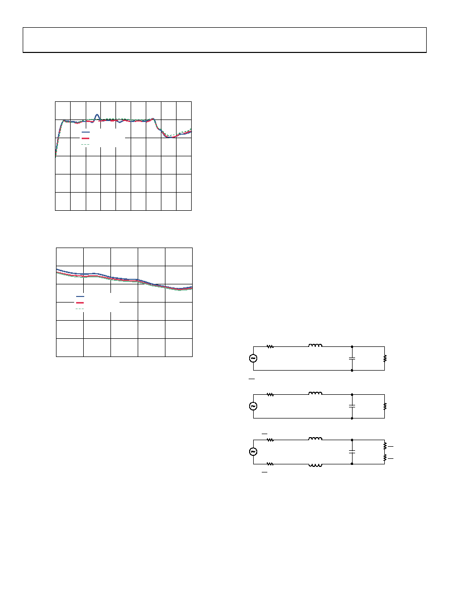
As an example, a second-order Butterworth, low-pass filter design
is shown in Figure 88 where the differential load impedance is
500 Ω and the source impedance of the ADL5380 is 50 Ω. The
normalized series inductor value for the 10-to-1, load-to-source
impedance ratio is 0.074 H, and the normalized shunt capacitor
is 14.814 F. For a 10.9 MHz cutoff frequency, the single-ended
equivalent circuit consists of a 0.54 μH series inductor followed
by a 433 pF shunt capacitor.
The balanced configuration is realized as the 0.54 μH inductor
is split in half to realize the network shown in Figure 88.
VS
RS
2
RS
RL
RS
2
RL
2
RL
2
433pF
VS
RS = 50
RL= 500
0.54H
0.27H
433pF
BALANCED
CONFIGURATION
DENORMALIZED
SINGLE-ENDED
EQUIVALENT
VS
RS = 50
= 0.1
RL= 500
LN = 0.074H
CN
14.814F
NORMALIZED
SINGLE-ENDED
CONFIGURATION
= 25
= 250
fC = 10.9MHz
fC = 1Hz
0
75
85
-08
7
Figure 88. Second-Order Butterworth, Low-Pass Filter Design Example
相關(guān)PDF資料 |
PDF描述 |
|---|---|
| ADL5504ACBZ-P2 | 450 MHz - 6000 MHz RF/MICROWAVE LINEAR DETECTOR |
| ADL5504ACBZ-P7 | 450 MHz - 6000 MHz RF/MICROWAVE LINEAR DETECTOR |
| ADL5535ARKZ-R7 | 20 MHz - 1000 MHz RF/MICROWAVE WIDE BAND LOW POWER AMPLIFIER |
| ADL5571 | 2500 MHz - 2700 MHz RF/MICROWAVE NARROW BAND MEDIUM POWER AMPLIFIER |
| ADRF6704ACPZ | 2500 MHz - 2900 MHz RF/MICROWAVE I/Q MODULATOR |
相關(guān)代理商/技術(shù)參數(shù) |
參數(shù)描述 |
|---|---|
| ADL5380-EVALZ | 功能描述:EVAL BOARD FOR ADL5380 制造商:analog devices inc. 系列:- 零件狀態(tài):有效 類型:解調(diào)器 頻率:400MHz ~ 6GHz 配套使用產(chǎn)品/相關(guān)產(chǎn)品:ADL5380 所含物品:板 標(biāo)準(zhǔn)包裝:1 |
| ADL5380XCPZ | 制造商:Analog Devices 功能描述: |
| ADL5382 | 制造商:AD 制造商全稱:Analog Devices 功能描述:700 MHz to 2.7 GHz Quadrature Demodulator |
| ADL5382ACPZ-R7 | 功能描述:IC DEMOD QUAD 700M2.7GHZ 24LFCSP RoHS:是 類別:RF/IF 和 RFID >> RF 解調(diào)器 系列:- 產(chǎn)品培訓(xùn)模塊:Lead (SnPb) Finish for COTS Obsolescence Mitigation Program 標(biāo)準(zhǔn)包裝:2,500 系列:- 功能:解調(diào)器 LO 頻率:- RF 頻率:70MHz ~ 300MHz P1dB:-9dBm 增益:- 噪音數(shù)據(jù):6.36dB 電流 - 電源:41.5mA 電源電壓:2.7 V 封裝/外殼:28-WFQFN 裸露焊盤 供應(yīng)商設(shè)備封裝:28-TQFN-EP(5x5) 包裝:帶卷 (TR) |
| ADL5382ACPZ-WP | 制造商:Analog Devices 功能描述:ADL5382: 700 MHZ TO 2700MHZ QUADRATURE DEMODULATOR - Waffle Pack |
發(fā)布緊急采購,3分鐘左右您將得到回復(fù)。