- 您現(xiàn)在的位置:買賣IC網(wǎng) > PDF目錄373993 > ADL5375 (Analog Devices, Inc.) 400 MHz to 6 GHz Broadband Quadrature Modulator PDF資料下載
參數(shù)資料
| 型號: | ADL5375 |
| 廠商: | Analog Devices, Inc. |
| 英文描述: | 400 MHz to 6 GHz Broadband Quadrature Modulator |
| 中文描述: | 400 MHz至6 GHz的寬帶正交調(diào)制器 |
| 文件頁數(shù): | 22/32頁 |
| 文件大小: | 1074K |
| 代理商: | ADL5375 |
第1頁第2頁第3頁第4頁第5頁第6頁第7頁第8頁第9頁第10頁第11頁第12頁第13頁第14頁第15頁第16頁第17頁第18頁第19頁第20頁第21頁當(dāng)前第22頁第23頁第24頁第25頁第26頁第27頁第28頁第29頁第30頁第31頁第32頁
ADL5375
OPTIMIZATION
The carrier feedthrough and sideband suppression performance of
the ADL5375 can be improved by using optimization techniques.
Carrier Feedthrough Nulling
Carrier feedthrough results from minute dc offsets that occur
between each of the differential baseband inputs. In an ideal
modulator, the quantities (V
IBBP
V
IBBN
) and (V
QBBP
V
QBBN
)
are equal to zero, which results in no carrier feedthrough. In a real
modulator, those two quantities are nonzero and, when mixed
with the LO, result in a finite amount of carrier feedthrough. The
ADL5375 is designed to provide a minimal amount of carrier
feedthrough. Should even lower carrier feedthrough levels be
required, minor adjustments can be made to the (V
IBBP
V
IBBN
)
and (V
QBBP
V
QBBN
) offsets. The I-channel offset is held constant,
while the Q-channel offset is varied until a minimum carrier
feedthrough level is obtained. The Q-channel offset required to
achieve this minimum is held constant, while the offset on the
I-channel is adjusted until a new minimum is reached. Through
two iterations of this process, the carrier feedthrough can be
reduced to as low as the output noise. The ability to null is
sometimes limited by the resolution of the offset adjustment.
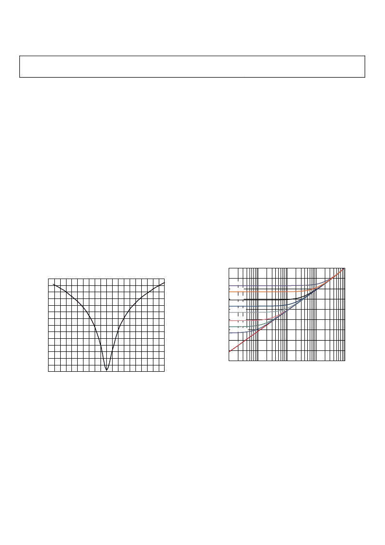
Figure 55 illustrates the typical relationship between carrier
feedthrough and dc offset around the null.
Rev. 0 | Page 22 of 32
–60
–88
–84
–80
–76
–72
–68
–64
–300 –240 –180 –120
–60
0
60
120
180
240
300
C
V
P
– V
N
OFFSET (μV)
0
Figure 55. Example of Typical Carrier Feedthrough vs. DC Offset Voltage
Using the ADL5375-05 version as an example, note that
throughout the nulling process, the dc bias for the base-
band inputs remains at 500 mV. When no offset is applied,
V
IBBP
=
V
IBBN
= 500 mV
,
or
V
IBBP
V
IBBN
=
V
IOS
= 0 V
When an offset of +V
IOS
is applied to the I-channel inputs,
V
IBBP
= 500 mV +
V
IOS
/2
,
and
V
IBBN
= 500 mV
V
IOS
/2
,
such
that
V
IBBP
V
IBBN
=
V
IOS
The same applies to the Q-channel. For the ADL5375-15, the
same theory applies except that
V
IBBP
=
V
IBBN
= 1500 mV
.
It is often desirable to perform a one-time carrier null calibra-
tion. This is usually performed at a given frequency and the
radio allowed to operate over a frequency range on each side
of that frequency. The nulled carrier feedthrough level degrades
somewhat as the LO frequency is moved away from the
frequency at which the null was performed. This variation is
very small across a 30 MHz or 60 MHz cellular band, however.
This small variation is due to the effects of LO-to-RF output
leakage around the package and on the board as the frequency
changes. Despite the degradation, the LO leakage can be
expected to be better than when no nulling is performed.
Sideband Suppression Optimization
Sideband suppression results from relative gain and relative
phase offsets between the I-channel and Q-channel and can
be suppressed through adjustments to those two parameters.
Figure 56 illustrates how sideband suppression is affected by
the gain and phase imbalances.
0dB
0.0125dB
0.025dB
0.05dB
0.125dB
0.25dB
0.5dB
1.25dB
2.5dB
0
–10
–20
–30
–40
–50
–60
–70
–80
–90
0.01
0.1
1
10
100
S
PHASE ERROR (Degrees)
0
Figure 56. Sideband Suppression vs. Quadrature Phase Error for
Various Quadrature Amplitude Offsets
Figure 56 underlines the fact that adjusting only one parameter
improves the sideband suppression only to a point, unless the
other parameter is also adjusted. For example, if the amplitude
offset is 0.25 dB, improving the phase imbalance by better than
1° does not yield any improvement in the sideband suppression.
For optimum sideband suppression, an iterative adjustment
between phase and amplitude is required.
The sideband suppression nulling can be performed either
through adjusting the gain for each channel or through the
modification of the phase and gain of the digital data coming
from the baseband signal processor.
相關(guān)PDF資料 |
PDF描述 |
|---|---|
| ADL5375-05ACPZ-R71 | 400 MHz to 6 GHz Broadband Quadrature Modulator |
| ADL5375-05-EVALZ1 | 400 MHz to 6 GHz Broadband Quadrature Modulator |
| ADL5375-15ACPZ-R71 | 400 MHz to 6 GHz Broadband Quadrature Modulator |
| ADL5375-15ACPZ-WP1 | 400 MHz to 6 GHz Broadband Quadrature Modulator |
| ADL5375-15-EVALZ1 | 400 MHz to 6 GHz Broadband Quadrature Modulator |
相關(guān)代理商/技術(shù)參數(shù) |
參數(shù)描述 |
|---|---|
| ADL5375_13 | 制造商:AD 制造商全稱:Analog Devices 功能描述:400 MHz to 6 GHz Broadband Quadrature Modulator |
| ADL5375-05 | 制造商:AD 制造商全稱:Analog Devices 功能描述:Interfacing the ADL5375 I/Q Modulator to the AD9779A Dual-Channel, 1 GSPS High Speed DAC |
| ADL5375-05ACPZ | 制造商:Analog Devices 功能描述:IC 400MHZ-6GHZ MOD QUAD 24LFCSP 制造商:Analog Devices 功能描述:IC, 400MHZ-6GHZ, MOD, QUAD, 24LFCSP 制造商:Analog Devices 功能描述:IC, 400MHZ-6GHZ, MOD, QUAD, 24LFCSP; Frequency Min:400MHz; Frequency Max:6GHz; RF Type:Quadrature; Supply Voltage Min:4.75V; Supply Voltage Max:5.25V; RF IC Case Style:LFCSP; No. of Pins:24; Operating Temperature Min:-40C; Operating;RoHS Compliant: Yes 制造商:Analog Devices 功能描述:Quadrature Mod 24-Pin LFCSP EP T/R |
| ADL5375-05ACPZ-R2 | 制造商:Analog Devices 功能描述:400 MHZ TO 6 GHZ BROADBAND QUADRATURE MODULATOR - Tape and Reel |
| ADL5375-05ACPZ-R7 | 功能描述:IC MOD QUAD 400MHZ-6GHZ 24LFCSP RoHS:是 類別:RF/IF 和 RFID >> RF 調(diào)制器 系列:- 產(chǎn)品培訓(xùn)模塊:Lead (SnPb) Finish for COTS Obsolescence Mitigation Program 標(biāo)準(zhǔn)包裝:2,500 系列:- 功能:調(diào)制器 LO 頻率:700MHz ~ 2.3GHz RF 頻率:700MHz ~ 2.3GHz P1dB:1dBm 底噪:-148dBm/Hz 輸出功率:-1dBm 電流 - 電源:46mA 電源電壓:2.7 V ~ 3.6 V 測試頻率:1.75GHz 封裝/外殼:28-WFQFN 裸露焊盤 包裝:帶卷 (TR) |
發(fā)布緊急采購,3分鐘左右您將得到回復(fù)。