- 您現(xiàn)在的位置:買賣IC網(wǎng) > PDF目錄373980 > ADE7760ARSRL (ANALOG DEVICES INC) Energy Metering IC with On-Chip Fault Detection PDF資料下載
參數(shù)資料
| 型號: | ADE7760ARSRL |
| 廠商: | ANALOG DEVICES INC |
| 元件分類: | 模擬信號調(diào)理 |
| 英文描述: | Energy Metering IC with On-Chip Fault Detection |
| 中文描述: | SPECIALTY ANALOG CIRCUIT, PDSO20 |
| 封裝: | MO-150AE, SSOP-20 |
| 文件頁數(shù): | 17/24頁 |
| 文件大小: | 514K |
| 代理商: | ADE7760ARSRL |
ADE7760
Note that if the on-chip reference is used, actual output
frequencies may vary from device to device due to reference
tolerance of ±8%.
Rev. 0 | Page 17 of 24
Hz
0
22
64
Hz
34
.
5
×
2
2
=
Hz
72
.
2
66
.
66
.
70
.
×
=
=
×
×
×
×
=
2
1
2
1
F
F
Frequency
As can be seen from these two example calculations, the
maximum output frequency for ac inputs is always half of that
for dc input signals. Table 7 shows a complete listing of all
maximum output frequencies for ac signals.
CF
Frequency
F
F
Table 7. Maximum Output Frequency on CF, F1, and F2 for
AC inputs
F1, F2 Maximum
Frequency
(Hz)
1
0
0
0.34
0
0
0
0.34
1
0
1
0.68
0
0
1
0.68
1
1
0
1.36
0
1
0
1.36
1
1
1
2.72
0
1
1
2.72
FAULT DETECTION
The ADE7760 incorporates a novel fault detection scheme that
warns of fault conditions and allows the ADE7760 to continue
accurate billing during a fault event. The ADE7760 does this by
continuously monitoring both the phase and neutral (return)
currents. A fault is indicated when these currents differ by more
than 6.25%. However, even during a fault, the output pulse rate
on F1 and F2 is generated using the larger of the two currents.
Because the ADE7760 looks for a difference between the voltage
signals on V
1A
and V
1B
, it is important that both current
transducers be closely matched.
SCF
S1
S0
CF Maximum
Frequency
(Hz)
43.52
21.76
43.52
21.76
43.52
21.76
43.52
5570
CF to
F1
Ratio
128
64
64
32
32
16
16
2048
On power-up, the output pulse rate of the ADE7760 is pro-
portional to the product of the voltage signals on V
1A
and
Channel 2. If there is a difference of greater than 6.25% between
V
1A
and V
1B
on power-up, the fault indicator (FAULT) becomes
active after about 1 s. In addition, if V
1B
is greater than V
1A
, the
ADE7760 selects V
1B
as the input. The fault detection is
automatically disabled when the voltage signal on Channel 1 is
less than 0.3% of the full-scale input range. This eliminates false
detection of a fault due to noise at light loads.
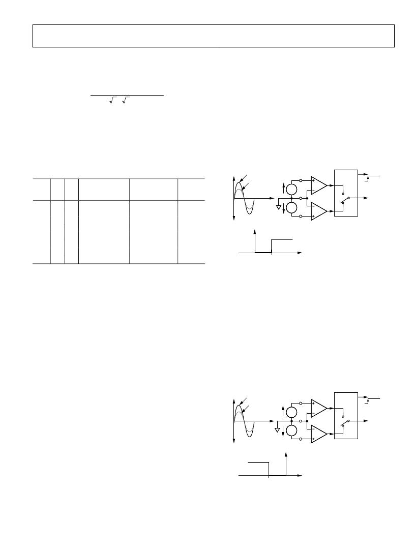
Fault with Active Input Greater than Inactive Input
If V
1A
is the active current input (that is, is being used for
billing), and the voltage signal on V
1B
(inactive input) falls below
93.75% of V
1A
, the fault indicator becomes active. Both analog
inputs are filtered and averaged to prevent false triggering of
this logic output. As a consequence of the filtering, there is a
time delay of approximately 3 s on the logic output FAULT after
the fault event. The FAULT logic output is independent of any
activity on outputs F1 or F2. Figure 23 shows one condition
under which FAULT becomes active. Because V
1A
is the active
input and it is still greater than V
1B
, billing is maintained on V
1A
,
that is, no swap to the V
1B
input occurs. V
1A
remains the active
input.
V
1B
V
1N
V
1A
AGND
FILTER
AND
COMPARE
TO
MULTIPLIER
FAULT
A
B
V
1A
V
1B
V
1B
< 93.75% OF V
1A
>0
<0
ACTIVE POINT – INACTIVE INPUT
6.25% OF ACTIVE INPUT
0
0V
FAULT
V
1A
V
1B
Figure 23. Fault Conditions for Active Input Greater than Inactive Input
Fault with Inactive Input Greater than Active Input
Figure 24 illustrates another fault condition. If the difference
between V
1B
, the inactive input, and V
1A
, the active input (used
for billing), becomes greater than 6.25% of V
1B
, the FAULT
indicator goes active, and there is also a swap over to the V
1B
input. The analog input V
1B
becomes the active input. Again,
there is a time constant of about 3 s associated with this swap.
V
1A
does not swap back to being the active channel until V
1A
is
greater than V
1B
and the difference between V
1A
and V
1B
—in this
order—becomes greater than 6.25% of V
1A
. The FAULT
indicator, however, becomes inactive as soon as V
1A
is within
6.25% of V
1B
. This threshold eliminates potential chatter
between V
1A
and V
1B
.
V
1B
V
1N
V
1A
AGND
FILTER
AND
COMPARE
TO
MULTIPLIER
FAULT
A
B
V
1A
V
1B
V
1A
< 93.75% OF V
1B
>0
<0
ACTIVE POINT – INACTIVE INPUT
6.25% OF INACTIVE INPUT
0
0V
FAULT + SWAP
V
1A
V
1B
Figure 24. Fault Conditions for Inactive Input Greater than Active Input
相關(guān)PDF資料 |
PDF描述 |
|---|---|
| ADE7760 | 8-Channel 14-Bit Single-Supply Voltage-Output DAC; Package: LQFP (10x10mm); No of Pins: 52; Temperature Range: Industrial |
| ADE7760ARS | Energy Metering IC with On-Chip Fault Detection |
| ADE7762 | Polyphase Energy Metering IC with Phase Drop Indication |
| ADE7762ARW | Polyphase Energy Metering IC with Phase Drop Indication |
| ADE7762ARW-RL | Polyphase Energy Metering IC with Phase Drop Indication |
相關(guān)代理商/技術(shù)參數(shù) |
參數(shù)描述 |
|---|---|
| ADE7761 | 制造商:AD 制造商全稱:Analog Devices 功能描述:Energy Metering IC with On-Chip Fault and Missing Neutral Detection |
| ADE7761A | 制造商:AD 制造商全稱:Analog Devices 功能描述:Energy Metering IC with On-Chip Fault and Missing Neutral Detection |
| ADE7761AARS | 制造商:Analog Devices 功能描述:Energy Measurement 20-Pin SSOP 制造商:Rochester Electronics LLC 功能描述: |
| ADE7761AARS-REF | 制造商:AD 制造商全稱:Analog Devices 功能描述:Energy Metering IC with On-Chip Fault and Missing Neutral Detection |
| ADE7761AARS-RL | 制造商:Analog Devices 功能描述:Energy Measurement 20-Pin SSOP T/R |
發(fā)布緊急采購,3分鐘左右您將得到回復(fù)。