- 您現(xiàn)在的位置:買賣IC網(wǎng) > PDF目錄373980 > ADE7755AN-REF (Analog Devices, Inc.) Energy Metering IC with Pulse Output PDF資料下載
參數(shù)資料
| 型號: | ADE7755AN-REF |
| 廠商: | Analog Devices, Inc. |
| 英文描述: | Energy Metering IC with Pulse Output |
| 中文描述: | 電能計(jì)量IC輸出脈沖 |
| 文件頁數(shù): | 12/16頁 |
| 文件大?。?/td> | 331K |
| 代理商: | ADE7755AN-REF |
REV. 0
ADE7755
–12–
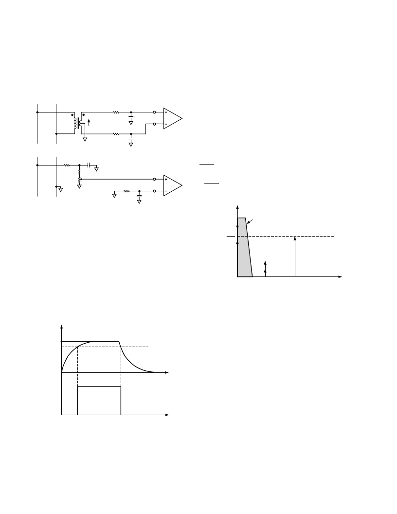
Figure 7 shows two typical connections for Channel V2. The first
option uses a PT (potential transformer) to provide complete
isolation from the power line. In the second option, the
ADE7755 is biased around the neutral wire, and a resistor divider
provides a voltage signal that is proportional to the line voltage.
Adjusting the ratio of Ra, Rb, and VR is also a convenient way of
carrying out a gain calibration on the meter.
660mV
Ra
*
Rb
*
VR
*
V2P
AGND
Rf
Rf
CT
NEUTRAL
PHASE
V2N
Cf
Cf
660mV
V2P
Rf
NEUTRAL
PHASE
V2N
Cf
Cf
*
Ra >> Rb + VR
*
Rb + VR = Rf
Figure 7. Typical Connections for Channel 2
POWER SUPPLY MONITOR
The ADE7755 contains an on-chip power supply monitor. The
Analog Supply (AV
DD
) is continuously monitored by the ADE7755.
If the supply is less than 4 V
±
5%, the ADE7755 will be reset.
This is useful to ensure correct device startup at power-up and
power-down. The power supply monitor has built in hysteresis
and filtering. This gives a high degree of immunity to false trig-
gering due to noisy supplies.
In Figure 8, the trigger level is nominally set at 4 V. The toler-
ance on this trigger level is about
±
5%. The power supply and
decoupling for the part should be such that the ripple at AV
DD
does not exceed 5 V
±
5% as specified for normal operation.
AV
DD
5V
4V
0V
INTERNAL
RESET
TIME
ACTIVE
RESET
Figure 8. On-Chip Power Supply Monitor
HPF and Offset Effects
Figure 9 shows the effect of offsets on the real power calculation.
An offset on Channel 1 and Channel 2 will contribute a dc
component after multiplication. Since the dc component is
extracted by the LPF, it will accumulate as real power. If not
properly filtered, dc offsets will introduce error to the energy
accumulation. This problem is easily avoided by enabling the
HPF (i.e., Pin AC/
DC
is set logic high) in Channel 1. By
removing the offset from at least one channel, no error compo-
nent can be generated at dc by the multiplication. Error terms
at cos(
w
t) are removed by the LPF and the digital-to-frequency
conversion (see Digital-to-Frequency Conversion section).
V
{
t
V
I
t
I
V
I
V
I
V
I
t
I
V
t
V
I
t
OS
OS
OS
OS
OS
OS
cos
cos
cos
cos
cos
w
w
w
w
w
( )
+
}
¥
( )
+
{
}
=
¥
2
+
¥
+
¥
( )
+
¥
( )
+
¥
2
¥
(
)
2
V
OS
I
OS
I
OS
V
V
OS
I
DC COMPONENT (INCLUDING ERROR TERM)
IS EXTRACTED BY THE LPF FOR REAL
POWER CALCULATION
2
FREQUENCY – RAD/S
2
V I
0
Figure 9. Effect of Channel Offset on the Real Power
Calculation
The HPF in Channel 1 has an associated phase response that is
compensated for on-chip. The phase compensation is activated
when the HPF is enabled and is disabled when the HPF is not
activated. Figures 10 and 11 show the phase error between chan-
nels with the compensation network activated. The ADE7755 is
phase compensated up to 1kHz as shown. This will ensure correct
active harmonic power calculation even at low power factors.
相關(guān)PDF資料 |
PDF描述 |
|---|---|
| ADE7755ARSRL | Energy Metering IC with Pulse Output |
| ADE7755 | Energy Metering IC with Pulse Output |
| ADE7755ARS | Energy Metering IC with Pulse Output |
| ADE7756EB | Evaluation Board Documentation AD7756 Energy metering IC |
| ADE7756 | Active Energy Metering IC with Serial Interface |
相關(guān)代理商/技術(shù)參數(shù) |
參數(shù)描述 |
|---|---|
| ADE7755ARS | 制造商:Analog Devices 功能描述:Energy Measurement 24-Pin SSOP 制造商:Rochester Electronics LLC 功能描述:ENERGY METERING IC WITH PULSE OUTPUT - Bulk 制造商:Analog Devices 功能描述:IC ENERGY METER 制造商:Maxim Integrated Products 功能描述:POWER METERING, 24 Pin, Plastic, SSOP |
| ADE7755ARSRL | 制造商:Analog Devices 功能描述:Energy Measurement 24-Pin SSOP T/R 制造商:Analog Devices 功能描述:IC ENERGY METER |
| ADE7755ARSRLZ | 制造商:AD 制造商全稱:Analog Devices 功能描述:Energy Metering IC with Pulse Output |
| ADE7755ARSRLZ1 | 制造商:AD 制造商全稱:Analog Devices 功能描述:Energy Metering IC with Pulse Output |
| ADE7755ARSZ | 功能描述:IC ENERGY METERING 1PHASE 24SSOP RoHS:是 類別:集成電路 (IC) >> PMIC - 能量測量 系列:- 產(chǎn)品培訓(xùn)模塊:Lead (SnPb) Finish for COTS Obsolescence Mitigation Program 標(biāo)準(zhǔn)包裝:2,500 系列:* |
發(fā)布緊急采購,3分鐘左右您將得到回復(fù)。