- 您現(xiàn)在的位置:買賣IC網(wǎng) > PDF目錄373980 > ADE7751ARS (ANALOG DEVICES INC) Energy Metering IC with On-Chip Fault Detection PDF資料下載
參數(shù)資料
| 型號(hào): | ADE7751ARS |
| 廠商: | ANALOG DEVICES INC |
| 元件分類: | 模擬信號(hào)調(diào)理 |
| 英文描述: | Energy Metering IC with On-Chip Fault Detection |
| 中文描述: | SPECIALTY ANALOG CIRCUIT, PDSO24 |
| 封裝: | SSOP-24 |
| 文件頁數(shù): | 12/16頁 |
| 文件大?。?/td> | 422K |
| 代理商: | ADE7751ARS |
REV. 0
ADE7751
–12–
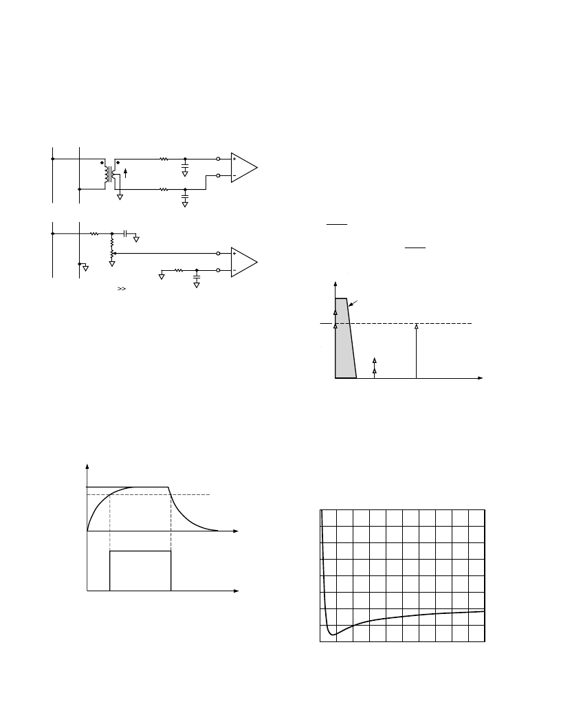
Figure 7 shows two typical connections for Channel V2. The first
option uses a PT (potential transformer) to provide complete isola-
tion from the mains voltage. In the second option, the ADE7751
is biased around the neutral wire and a resistor divider is used to
provide a voltage signal that is proportional to the line voltage.
Adjusting the ratio of Ra and Rb is also a convenient way of
carrying out a gain calibration on the meter.
660mV
Ra
Rb
VR
V2P
AGND
Rf
Rf
CT
NEUTRAL
PHASE
V2N
Cf
Cf
660mV
V2P
Rf
NEUTRAL
PHASE
V2N
Cf
Cf
NOTE
Ra
Rb + VR = Rf
Rf;
Figure 7. Typical Connections for Channel 2
POWER SUPPLY MONITOR
The ADE7751 contains an on-chip power supply monitor. The
analog supply (AV
DD
) is continuously monitored by the ADE7751.
If the supply is less than 4 V
±
5%, the ADE7751 will be reset.
This is useful to ensure correct device start up at power-up and
power-down. The power supply monitor has built-in hysteresis
and filtering. This gives a high degree of immunity to false
triggering due to noisy supplies.
As can be seen in Figure 8, the trigger level is nominally set at 4 V.
The tolerance on this trigger level is about
±
5%. The power supply
and decoupling for the part should be such that the ripple at AV
DD
does not exceed 5 V
±
5% as specified for normal operation.
AV
DD
5V
4V
0V
INTERNAL
RESET
RESET
TIME
ACTIVE
RESET
Figure 8. On-Chip Power Supply Monitor
HPF and Offset Effects
Figure 9 shows the effect of offsets on the real power calculation. As
shown in Figure 9, an offset on Channel 1 and Channel 2 will
contribute a dc component after multiplication. Since this dc
component is extracted by the LPF and used to generate the real
power information, the offsets will have contributed a constant
error to the real power calculation. This problem is easily avoided by
enabling the HPF (i.e., pin AC/
DC
is set logic high) in Channel 1.
By removing the offset from at least one channel, no error component
can be generated at dc by the multiplication. Error terms at cos(
ω
t)
are removed by the LPF and the digital-to-frequency conversion—
see Digital-to-Frequency Conversion section.
V
(
t
V
I
t
I
V
I
V
I
V
I
t
V
I
t
V
I
t
OS
OS
OS
OS
OS
OS
cos(
×
2
)
cos(
)
cos(
)
cos(
)
cos(
)
ω
ω
ω
ω
ω
+
)
×
×
+
(
)
=
+
×
+
×
×
+
×
×
+
×
2
×
2
V
OS
I
OS
I
OS
V
V
OS
I
DC COMPONENT (INCLUDING ERROR TERM)
IS EXTRACTED BY THE LPF FOR REAL
POWER CALCULATION
2
FREQUENCY – RAD/S
2
V I
0
Figure 9. Effect of Channel Offsets on the
Real Power Calculation
The HPF in Channel 1 has an associated phase response that is
compensated for on-chip. The phase compensation is activated
when the HPF is enabled and is disabled when the HPF is not
activated. Figures 10 and 11 show the phase error between chan-
nels with the compensation network activated. The ADE7751
is phase compensated up to 1 kHz as shown. This will ensure
correct active harmonic power calculation even at low-power factors.
FREQUENCY – Hz
0
100
P
–0.05
–0.10
0
0.05
0.10
0.15
0.20
0.25
0.30
200
300
400
500
600
700
800
900 1000
Figure 10. Phase Error Between Channels (0 Hz to 1 kHz)
相關(guān)PDF資料 |
PDF描述 |
|---|---|
| ADE7751ARSRL | Energy Metering IC with On-Chip Fault Detection |
| ADE7752B | Polyphase Energy Metering IC with Pulsed Output |
| ADE7752BARW | Polyphase Energy Metering IC with Pulsed Output |
| ADE7752BARW-RL | Polyphase Energy Metering IC with Pulsed Output |
| ADE7752BARWZ | Polyphase Energy Metering IC with Pulsed Output |
相關(guān)代理商/技術(shù)參數(shù) |
參數(shù)描述 |
|---|---|
| ADE7751ARSRL | 制造商:Analog Devices 功能描述:Energy Measurement 24-Pin SSOP T/R 制造商:Analog Devices 功能描述:IC ENERGY METER |
| ADE7751ARSZ | 功能描述:IC ENERGY METERING 1PHASE 24SSOP RoHS:是 類別:集成電路 (IC) >> PMIC - 能量測量 系列:- 產(chǎn)品培訓(xùn)模塊:Lead (SnPb) Finish for COTS Obsolescence Mitigation Program 標(biāo)準(zhǔn)包裝:2,500 系列:* |
| ADE7751ARSZRL | 功能描述:IC ENERGY METERING 1PHASE 24SSOP RoHS:是 類別:集成電路 (IC) >> PMIC - 能量測量 系列:- 產(chǎn)品培訓(xùn)模塊:Lead (SnPb) Finish for COTS Obsolescence Mitigation Program 標(biāo)準(zhǔn)包裝:2,500 系列:* |
| ADE7752 | 制造商:AD 制造商全稱:Analog Devices 功能描述:Three Phase Energy Metering IC with Pulse Output |
| ADE7752A | 制造商:AD 制造商全稱:Analog Devices 功能描述:Polyphase Energy Metering IC with Pulse Output |
發(fā)布緊急采購,3分鐘左右您將得到回復(fù)。