- 您現(xiàn)在的位置:買賣IC網(wǎng) > PDF目錄373980 > ADE7751AAN-REF (Analog Devices, Inc.) Energy Metering IC with On-Chip Fault Detection PDF資料下載
參數(shù)資料
| 型號: | ADE7751AAN-REF |
| 廠商: | Analog Devices, Inc. |
| 英文描述: | Energy Metering IC with On-Chip Fault Detection |
| 中文描述: | 電能計(jì)量IC片故障檢測 |
| 文件頁數(shù): | 15/16頁 |
| 文件大小: | 422K |
| 代理商: | ADE7751AAN-REF |
REV. 0
ADE7751
–15–
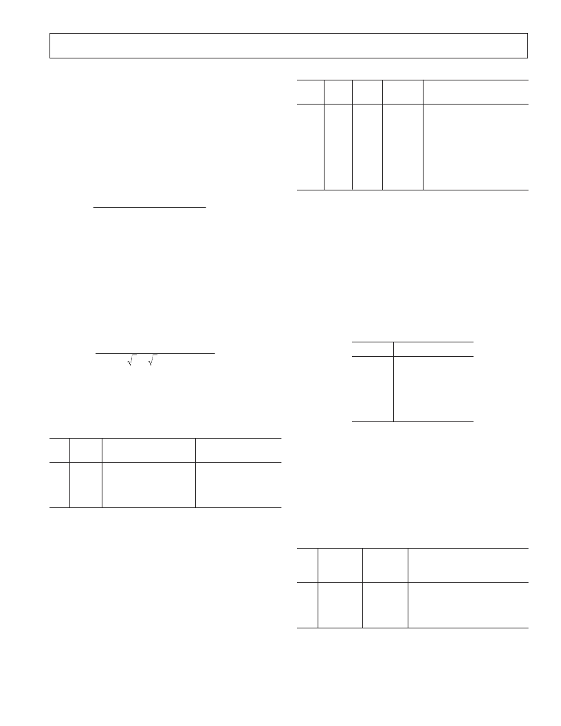
Table IV.
F
1–4
(Hz)
CF Max for AC Signals
(Hz)
128
×
F1, F2 = 43.52
64
×
F1, F2 = 21.76
64
×
F1, F2 = 43.52
32
×
F1, F2 = 21.76
32
×
F1, F2 = 43.52
16
×
F1, F2 = 21.76
16
×
F1, F2 = 43.52
8
×
F1, F2 = 21.76
SCF
S1
S0
1
0
1
0
1
0
1
0
0
0
0
0
1
1
1
1
0
0
1
1
0
0
1
1
1.7
1.7
3.4
3.4
6.8
6.8
13.6
13.6
SELECTING A FREQUENCY FOR AN ENERGY METER
APPLICATION
As shown in Table II, the user can select one of four frequencies.
This frequency selection determines the maximum frequency
on F1 and F2. These outputs are intended to be used to drive
the energy register (electromechanical or other). Since only four
different output frequencies can be selected, the available
frequency selection has been optimized for a meter constant of
100 imp/kWhr with a maximum current of between 10 A and
120 A. Table V shows the output frequency for several maximum
currents (I
MAX
) with a line voltage of 220 V. In all cases, the
meter constant is 100 imp/kWhr.
Table V.
I
MAX
12.5 A
25 A
40 A
60 A
80 A
120 A
F1 and F2 (Hz)
0.076
0.153
0.244
0.367
0.489
0.733
The F
1–4
frequencies allow complete coverage of this range of
output frequencies on F1 and F2. When designing an energy
meter, the nominal design voltage on Channel 2 (voltage) should
be set to half scale to allow for calibration of the meter constant.
The current channel should also be no more than half scale when the
meter sees maximum load. This will allow overcurrent signals and
signals with high crest factors to be accommodated. Table VI
shows the output frequency on F1 and F2 when both analog
inputs are half scale. The frequencies listed in Table VI align very
well with those listed in Table V for maximum load.
Table VI.
Frequency on F1 and F2 –
CH1 and CH2
Half-Scale AC Inputs
S1
S0
F
1–4
1.7
3.4
6.8
13.6
0
0
1
1
0
1
0
1
0.085 Hz
0.17 Hz
0.34 Hz
0.68 Hz
Example 1
If full-scale differential dc voltages of +660 mV and –660 mV are
applied to V1 and V2 respectively (660 mV is the maximum
differential voltage that can be connected to Channel 1 and
Channel 2), the expected output frequency is calculated as follows.
Gain
=
1, G0 = G1 = 0
F
1–4
=
1.7 Hz, S0 = S1 = 0
V1
=
+660 mV dc = 0.66 V (rms of dc = dc)
V2
=
–660 mV dc = 0.66 V (rms of dc = |dc|)
V
REF
=
2.5 V (nominal reference value)
Note: If the on-chip reference is used, actual output frequencies
may vary from device to device due to reference tolerance of
±
8%.
×
×
5 74
0 66
0 66 1 1 7
2 5
.
Freq
Hz
Hz
=
=
0 68
.
2
.
.
.
.
(8)
Example 2
In this example, if ac voltages of
±
660 mV peak are applied to
V1 and V2, the expected output frequency is calculated as follows.
Gain
= 1, G0
=
G1
=
0
F
1–4
= 1.7 Hz, S0
=
S1 = 0
V1
= rms of 660 mV peak ac = 0.66/
√
2
V
V2
= rms of 660 mV peak ac = 0.66/
√
2
V
V
REF
= 2.5 V (nominal reference value)
Note: If the on-chip reference is used, actual output frequencies
may vary from device to device due to reference tolerance of
±
8%.
Freq
Hz
Hz
=
×
×
×
×
2 5
.
×
×
=
5 74
.
0 66
.
0 66
.
1
1 7
.
2
2
0 34
.
2
(9)
As shown in these two example calculations, the maximum
output frequency for ac inputs is always half of that for dc
input signals. Table III shows a complete listing of all maxi-
mum output frequencies.
Table III.
Max Frequency
for DC Inputs (Hz)
Max Frequency
for AC Inputs (Hz)
S1
S0
0
0
1
1
0
1
0
1
0.68
1.36
2.72
5.44
0.34
0.68
1.36
2.72
Frequency Output CF
The pulse output CF (calibration frequency) is intended for use
during calibration. The output pulse rate on CF can be up to 128
times the pulse rate on F1 and F2. The lower the F
1–4
frequency
selected the higher the CF scaling. Table IV shows how the two
frequencies are related depending on the states of the logic inputs
S0, S1, and SCF. Because of its relatively high-pulse rate, the
frequency at this logic output is proportional to the instantaneous
real power. As is the case with F1 and F2, the frequency is derived
from the output of the low-pass filter after multiplication. However,
because the output frequency is high, this real power information
is accumulated over a much shorter time. Hence, less averaging
is carried out in the digital-to-frequency conversion. With much
less averaging of the real power signal, the CF output is much
more responsive to power fluctuations (see Figure 2).
相關(guān)PDF資料 |
PDF描述 |
|---|---|
| ADE7751AN | Energy Metering IC with On-Chip Fault Detection |
| ADE7751ARS | Energy Metering IC with On-Chip Fault Detection |
| ADE7751ARSRL | Energy Metering IC with On-Chip Fault Detection |
| ADE7752B | Polyphase Energy Metering IC with Pulsed Output |
| ADE7752BARW | Polyphase Energy Metering IC with Pulsed Output |
相關(guān)代理商/技術(shù)參數(shù) |
參數(shù)描述 |
|---|---|
| ADE7751AN | 制造商:Analog Devices 功能描述:Energy Measurement 24-Pin PDIP 制造商:Analog Devices 功能描述:ENERGY MEASUREMENT 24PDIP - Bulk 制造商:Rochester Electronics LLC 功能描述:PRODUCT TO FREQUENCY CONVERTER I.C. - Bulk |
| ADE7751ARS | 制造商:Rochester Electronics LLC 功能描述:PRODUCT TO FREQUENCY CONVERTER I.C. - Bulk 制造商:Analog Devices 功能描述:IC ENERGY METER |
| ADE7751ARSRL | 制造商:Analog Devices 功能描述:Energy Measurement 24-Pin SSOP T/R 制造商:Analog Devices 功能描述:IC ENERGY METER |
| ADE7751ARSZ | 功能描述:IC ENERGY METERING 1PHASE 24SSOP RoHS:是 類別:集成電路 (IC) >> PMIC - 能量測量 系列:- 產(chǎn)品培訓(xùn)模塊:Lead (SnPb) Finish for COTS Obsolescence Mitigation Program 標(biāo)準(zhǔn)包裝:2,500 系列:* |
| ADE7751ARSZRL | 功能描述:IC ENERGY METERING 1PHASE 24SSOP RoHS:是 類別:集成電路 (IC) >> PMIC - 能量測量 系列:- 產(chǎn)品培訓(xùn)模塊:Lead (SnPb) Finish for COTS Obsolescence Mitigation Program 標(biāo)準(zhǔn)包裝:2,500 系列:* |
發(fā)布緊急采購,3分鐘左右您將得到回復(fù)。