- 您現(xiàn)在的位置:買賣IC網(wǎng) > PDF目錄373979 > ADDC02812 (Analog Devices, Inc.) 28 V/100 W DC/DC Converters(帶積分EMI濾波器的DC-DC轉(zhuǎn)換器) PDF資料下載
參數(shù)資料
| 型號(hào): | ADDC02812 |
| 廠商: | Analog Devices, Inc. |
| 英文描述: | 28 V/100 W DC/DC Converters(帶積分EMI濾波器的DC-DC轉(zhuǎn)換器) |
| 中文描述: | 中西區(qū)區(qū)議會(huì)28 V/100 / DC轉(zhuǎn)換器(帶積分的EMI濾波器的的DC - DC轉(zhuǎn)換器) |
| 文件頁數(shù): | 12/20頁 |
| 文件大小: | 208K |
| 代理商: | ADDC02812 |
–12–
ADDC02812DA/ADDC02815DA
Incremental Negative Resistance
: A POL converter is designed
to hold its output voltage constant no matter how its input volt-
age varies. Given a constant load current, the power drawn from
the input bus is therefore also a constant. If the input voltage
increases by some factor, the input current must decrease by the
same factor to keep the power level constant. In incremental
terms, a positive incremental change in the input voltage results
in a negative incremental change in the input current. T he POL
converter therefore looks, incrementally, as a negative resistor.
T he value of this negative resistor at a particular operating
point, V
IN
, I
IN
, is:
R
N
=
±
V
IN
REV. A
I
IN
Note that this resistance is a function of the operating point. At
full load and low input line, the resistance is its smallest, while
at light load and high input line, it is its largest.
Potential System Instability
: T he preceding analysis assumes
dc voltages and currents. For ac waveforms the incremental input
model for the POL converter must also include the effects of its
input filter and control loop dynamics. When the POL con-
verter is connected to a power source, modeled as a voltage
source,
V
S
, in series with an inductor,
L
S
, and some positive
resistor,
R
S
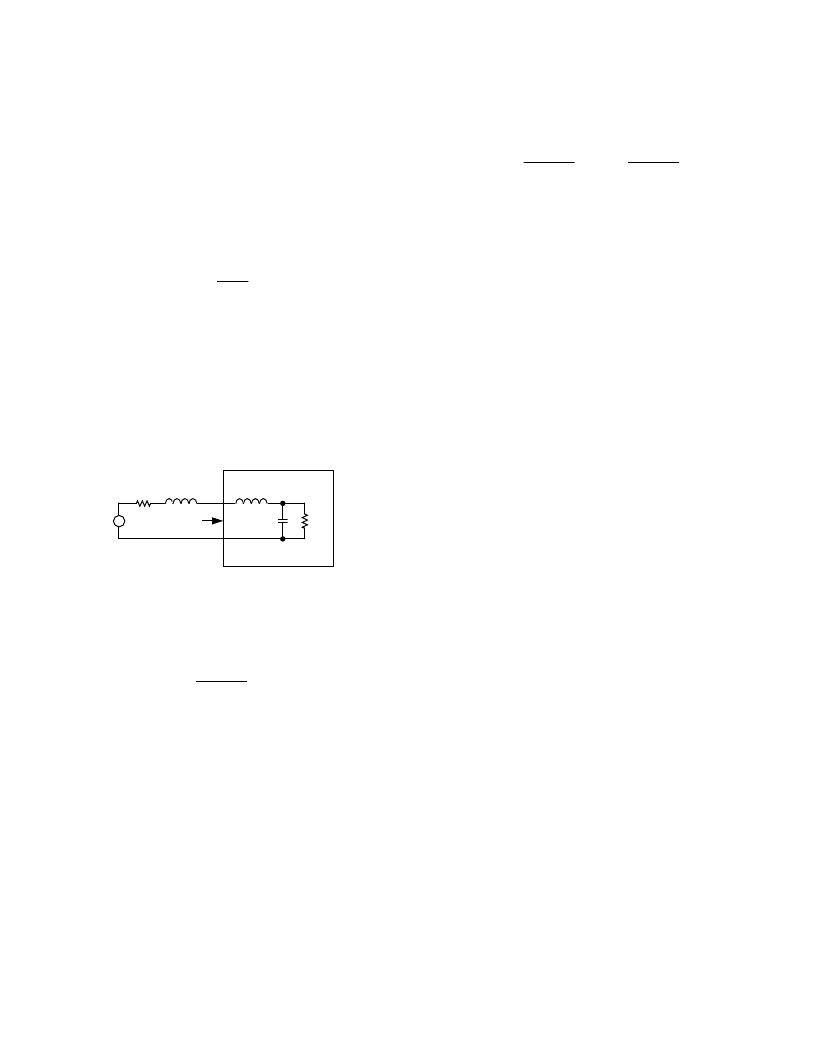
, the network of Figure 25 results.
L
P
C
P
–|R
N
|
ADI DC/DC CONVERTER
L
S
R
S
V
S
INPUT
TERMINALS
Figure 25. Model of Power Source and POL Converter
Connection
T he network shown in Figure 25 is second order and has the
following characteristic equation:
s
2
(
L
S
+
L
P
)
C
+
s
(
L
S
+
L
P
)
±|
R
N
|
+
R
S
C
P
+
1
=
0
For the power delivery to be efficient, it is required that R
S
<<
R
N
. For the system to be stable, however, the following relation-
ship must hold:
C
P
|
R
N
|
>
(
L
S
+
L
P
)
R
S
or
R
S
>
(
L
S
+
L
P
)
C
P
|
R
N
|
Notice from this result that if (L
S
+ L
P
) is too large, or if R
S
is
too small, the system might be unstable. T his condition would
first be observed at low input line and full load since the abso-
lute value of R
N
is smallest at this operating condition.
If an instability results and it cannot be corrected by changing
L
S
or R
S
, such as during the MIL-ST D-461D tests due to the
LISN requirement, one possible solution is to place a capacitor
across the input of the POL converter. Another possibility is to
place a small resistor in series with this extra capacitor.
T he analysis so far has assumed the source of power was a volt-
age source (e.g., a battery) with some source impedance. In
some cases, this source may be the output of a front-end (FE)
converter. Although each FE converter is different, a model for
a typical one would have an LC output filter driven by a voltage
source whose value was determined by the feedback loop. T he
LC filter usually has a high Q, so the compensation of the feed-
back loop is chosen to help dampen any oscillations that result
from load transients. In effect, the feedback loop adds “positive
resistance” to the LC network.
When the POL converter is connected to the output of this FE
converter, the POL’s “negative resistance” counteracts the
effects of the FE’s “positive resistance” offered by the feedback
loop. Depending on the specific details, this might simply mean
that the FE converter’s transient response is slightly more oscil-
latory, or it may cause the entire system to be unstable.
For the ADDC02812DA and ADDC02815DA, L
P
is approxi-
mately 1
μ
H and C
P
is approximately 4
μ
F. Figure 12 shows a
more accurate depiction of the input impedance of the converter
as a function of frequency. T he negative resistance is, itself, a
very good incremental model for the power state of the con-
verter for frequencies into the several kHz range (see Figure 12).
相關(guān)PDF資料 |
PDF描述 |
|---|---|
| ADDC02828SA | 28 V/100 W DC/DC Converter with Integral EMI Filter |
| ADDC02828SATV | 28 V/100 W DC/DC Converter with Integral EMI Filter |
| ADDC02828SAKV | JT 7C 7#20 PIN GRND PLUG |
| ADDC02828 | 270V/100W DC/DC Converter with Integral EMI Filter(帶積分EMI濾波器的DC-DC轉(zhuǎn)換器) |
| ADDS-21XX-EZLITE | RIBBON CABLE, RND/FLAT, 50WAY, PER M; Cores, No. of:50; Conductor make-up:7/36AWG; Impedance:75R; Pitch:1.27mm; Voltage rating, AC:300V; Colour:Grey; Approval Bodies:UL, CSA; Area, conductor CSA:0.072mm2; Cable UL style number:UL RoHS Compliant: Yes |
相關(guān)代理商/技術(shù)參數(shù) |
參數(shù)描述 |
|---|---|
| ADDC02812DA | 制造商:AD 制造商全稱:Analog Devices 功能描述:28 V/100 W DC/DC Converters with Integral EMI Filter |
| ADDC02812DAKV | 制造商:AD 制造商全稱:Analog Devices 功能描述:28 V/100 W DC/DC Converters with Integral EMI Filter |
| ADDC02812DATV | 制造商:AD 制造商全稱:Analog Devices 功能描述:28 V/100 W DC/DC Converters with Integral EMI Filter |
| ADDC02812DATV/883B | 制造商:未知廠家 制造商全稱:未知廠家 功能描述:DC-to-DC Voltage Converter |
| ADDC02812DATV/QMLH | 制造商:AD 制造商全稱:Analog Devices 功能描述:28 V/100 W DC/DC Converters with Integral EMI Filter |
發(fā)布緊急采購,3分鐘左右您將得到回復(fù)。