- 您現(xiàn)在的位置:買賣IC網(wǎng) > PDF目錄375252 > ADC71 16-Bit ANALOG-TO-DIGITAL CONVERTER PDF資料下載
參數(shù)資料
| 型號(hào): | ADC71 |
| 英文描述: | 16-Bit ANALOG-TO-DIGITAL CONVERTER |
| 中文描述: | 16位模擬數(shù)字轉(zhuǎn)換器 |
| 文件頁(yè)數(shù): | 3/9頁(yè) |
| 文件大小: | 96K |
| 代理商: | ADC71 |
3
ADC71
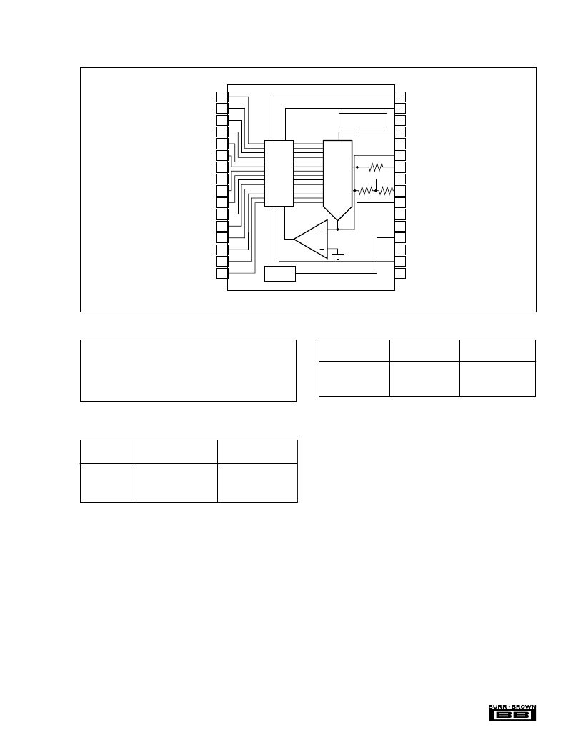
PIN CONFIGURATION
ABSOLUTE MAXIMUM SPECIFICATIONS
+V
CC
to Common.................................................................... 0 to +16.5V
–V
CC
to Common.................................................................. 0V to –16.5V
+V
to Common....................................................................... 0V to +7V
Analog Common to Digital Common ...............................................
±
0.5V
Logic Inputs to Common ........................................................... 0V to V
DD
Maximum Power Dissipation .......................................................1000mW
Lead Temperature (10s).................................................................. 300
°
C
PACKAGE INFORMATION
PACKAGE DRAWING
NUMBER
(1)
MODEL
PACKAGE
ADC71JG
ADC71KG
ADC71AG
ADC71BG
32-Pin Hermetic DIP
32-Pin Hermetic DIP
32-Pin Hermetic DIP
32-Pin Hermetic DIP
172-5
172-5
172-5
172-5
NOTE: (1) For detailed drawing and dimension table, please see end of data
sheet, or Appendix D of Burr-Brown IC Data Book.
Top View
DIP
ORDERING INFORMATION
MODEL
TEMPERATURE RANGE
NONLINEARITY
ADC71JG
ADC71KG
ADC71AG
ADC71BG
0
°
C to +70
°
C
0
°
C to +70
°
C
–25
°
C to +85
°
C
–25
°
C to +85
°
C
±
0.006% FSR
±
0.003% FSR
±
0.006% FSR
±
0.003% FSR
The information provided herein is believed to be reliable; however, BURR-BROWN assumes no responsibility for inaccuracies or omissions. BURR-BROWN assumes
no responsibility for the use of this information, and all use of such information shall be entirely at the user’s own risk. Prices and specifications are subject to change
without notice. No patent rights or licenses to any of the circuits described herein are implied or granted to any third party. BURR-BROWN does not authorize or warrant
any BURR-BROWN product for use in life support devices and/or systems.
NOTE: (1) Metal lid of package is connected to pin 22 (Analog Common).
Clock
Reference
C
32
31
30
29
28
27
26
25
24
23
22
21
20
19
18
17
1
2
3
4
5
6
7
8
9
10
11
12
13
14
15
16
(MSB) Bit 1
Bit 2
Bit 3
Bit 4
Bit 5
Bit 6
Bit 7
Bit 8
Bit 9
Bit 10
Bit 11
Bit 12
(LSB for 13 bits) Bit 13
(LSB for 14 bits) Bit 14
Bit 15
Bit 16
Short Cycle
Convert Command
+5VDC Supply
Gain Adjust
+15VDC Supply
Comparator In
Bipolar Offset
10V
20V
Ref Out 6.3V
Analog Common
(1)
–15VDC Supply
Clock Out
Digital Common
Status
Serial Out
6.3k
1
Comparator
5k
5k
相關(guān)PDF資料 |
PDF描述 |
|---|---|
| ADC71AG | 16-Bit ANALOG-TO-DIGITAL CONVERTER |
| ADC71BG | 16-Bit ANALOG-TO-DIGITAL CONVERTER |
| ADC71JG | 16-Bit ANALOG-TO-DIGITAL CONVERTER |
| ADC71KG | 16-Bit ANALOG-TO-DIGITAL CONVERTER |
| ADC72 | 16 BIT HYBRID ANALOG TO DIGITAL CONVERTER |
相關(guān)代理商/技術(shù)參數(shù) |
參數(shù)描述 |
|---|---|
| ADC71006701 | 制造商:LG Corporation 功能描述:Door Assembly,Freezer |
| ADC71006702 | 制造商:LG Corporation 功能描述:Door Assembly,Freezer |
| ADC71006703 | 制造商:LG Corporation 功能描述:Door Assembly,Freezer |
| ADC71006704 | 制造商:LG Corporation 功能描述:Door Assembly,Freezer |
| ADC71006705 | 制造商:LG Corporation 功能描述:Door Assembly,Freezer |
發(fā)布緊急采購(gòu),3分鐘左右您將得到回復(fù)。