- 您現(xiàn)在的位置:買賣IC網(wǎng) > PDF目錄17064 > AD9767-EBZ (Analog Devices Inc)BOARD EVAL FOR AD9767 PDF資料下載
參數(shù)資料
| 型號: | AD9767-EBZ |
| 廠商: | Analog Devices Inc |
| 文件頁數(shù): | 18/44頁 |
| 文件大?。?/td> | 0K |
| 描述: | BOARD EVAL FOR AD9767 |
| 產(chǎn)品培訓(xùn)模塊: | DAC Architectures |
| 標(biāo)準(zhǔn)包裝: | 1 |
| 系列: | TxDAC+® |
| DAC 的數(shù)量: | 2 |
| 位數(shù): | 14 |
| 采樣率(每秒): | 125M |
| 數(shù)據(jù)接口: | 并聯(lián) |
| 設(shè)置時間: | 35ns |
| DAC 型: | 電流 |
| 工作溫度: | -40°C ~ 85°C |
| 已供物品: | 板 |
| 已用 IC / 零件: | AD9767 |
| 相關(guān)產(chǎn)品: | AD9767ASTZRL-ND - IC DAC 14BIT DUAL 125MSPS 48LQFP AD9767ASTZ-ND - IC DAC 14BIT DUAL 125MSPS 48LQFP |
第1頁第2頁第3頁第4頁第5頁第6頁第7頁第8頁第9頁第10頁第11頁第12頁第13頁第14頁第15頁第16頁第17頁當(dāng)前第18頁第19頁第20頁第21頁第22頁第23頁第24頁第25頁第26頁第27頁第28頁第29頁第30頁第31頁第32頁第33頁第34頁第35頁第36頁第37頁第38頁第39頁第40頁第41頁第42頁第43頁第44頁
Data Sheet
AD9763/AD9765/AD9767
Rev. G | Page 25 of 44
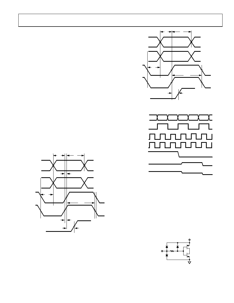
Interleaved Mode Timing
When the MODE pin is at Logic 0, the AD9763/AD9765/AD9767
operate in interleaved mode (refer to Figure 61). In addition,
WRT1 functions as IQWRT, CLK1 functions as IQCLK, WRT2
functions as IQSEL, and CLK2 functions as IQRESET.
Data enters the device on the rising edge of IQWRT. The logic level
of IQSEL steers the data to either Channel Latch 1 (IQSEL = 1) or
to Channel Latch 2 (IQSEL = 0). For proper operation, IQSEL
must change state only when IQWRT and IQCLK are low.
When IQRESET is high, IQCLK is disabled. When IQRESET
goes low, the next rising edge on IQCLK updates both DAC
latches with the data present at their inputs. In the interleaved
mode, IQCLK is divided by 2 internally. Following this first
rising edge, the DAC latches are only updated on every other
rising edge of IQCLK. In this way, IQRESET can be used to
synchronize the routing of the data to the DACs.
Similar to the order of CLK and WRT in dual-port mode,
IQCLK must occur before or simultaneously with IQWRT.
Timing specifications for interleaved mode are shown in Figure 64
and Figure 66.
The digital inputs are CMOS compatible with logic thresholds,
VTHRESHOLD, set to approximately half the digital positive supply
(DVDDx), or
VTHRESHOLD = DVDDx/2(±20%)
DATA IN
IQSEL
IQWRT
IQCLK
IOUTA
OR
IOUTB
*APPLIES TO FALLING EDGE OF IQCLK/IQWRT AND IQSEL ONLY.
500 ps
tS
tH
tPD
tLPW
tH*
00
61
7-
0
64
Figure 64. 5 V or 3.3 V Interleaved Mode Timing
At 5 V it is permissible to drive IQWRT and IQCLK together as
shown in Figure 65, but at 3.3 V the interleaved data transfer is
not reliable.
DATA IN
IQSEL
IQWRT
IQCLK
IOUTA
OR
IOUTB
*APPLIES TO FALLING EDGE OF IQCLK/IQWRT AND IQSEL ONLY.
tH*
tS
tH
tPD
tLPW
00
61
7-
0
65
Figure 65. 5 V Only Interleaved Mode Timing
IQSEL
IQWRT
IQCLK
IQRESET
xx
D1
D2
D3
D4
xx
D1
D2
D3
D4
D5
INTERLEAVED
DATA
DAC OUTPUT
PORT 1
DAC OUTPUT
PORT 2
00
617
-06
6
Figure 66. Interleaved Mode Timing
The internal digital circuitry of the AD9763/AD9765/AD9767
is capable of operating at a digital supply of 3.3 V or 5 V. As a
result, the digital inputs can also accommodate TTL levels when
DVDD1/DVDD2 is set to accommodate the maximum high
level voltage (VOH(MAX)) of the TTL drivers. A DVDD1/DVDD2
of 3.3 V typically ensures proper compatibility with bipolar TTL
logic families. Figure 67 shows the equivalent digital input
circuit for the data and clock inputs. The sleep mode input is
similar, with the exception that it contains an active pull-down
circuit, thus ensuring that the AD9763/AD9765/AD9767
remains enabled if this input is left disconnected.
DIGITAL
INPUT
DVDD1
00
61
7
-06
7
Figure 67. Equivalent Digital Input
相關(guān)PDF資料 |
PDF描述 |
|---|---|
| 0210490255 | CABLE JUMPER 1.25MM .030M 20POS |
| MLG1005S2N0S | INDUCTOR MULTILAYER 2.0NH 0402 |
| MIC2003-0.5YML TR | IC DISTRIBUTION SW 0.5A 6-MLF |
| MIC2005-0.5YM6 TR | IC DISTRIBUTION SW 0.5A SOT23-6 |
| 0210490204 | CABLE JUMPER 1.25MM .203M 14POS |
相關(guān)代理商/技術(shù)參數(shù) |
參數(shù)描述 |
|---|---|
| AD9768 | 制造商:AD 制造商全稱:Analog Devices 功能描述:Ultrahigh Speed IC D/A Converter |
| AD9768JD | 制造商:Rochester Electronics LLC 功能描述:AD9768 IC - Bulk |
| AD9768JQ | 制造商:Rochester Electronics LLC 功能描述:- Bulk |
| AD9768SD | 制造商:AD 制造商全稱:Analog Devices 功能描述:Ultrahigh Speed IC D/A Converter |
| AD9768SE | 制造商:Rochester Electronics LLC 功能描述:- Bulk |
發(fā)布緊急采購,3分鐘左右您將得到回復(fù)。