- 您現(xiàn)在的位置:買賣IC網(wǎng) > PDF目錄373963 > AD9444BSVZ-80 (ANALOG DEVICES INC) 14-Bit, 80 MSPS, A/D Converter PDF資料下載
參數(shù)資料
| 型號(hào): | AD9444BSVZ-80 |
| 廠商: | ANALOG DEVICES INC |
| 元件分類: | ADC |
| 英文描述: | 14-Bit, 80 MSPS, A/D Converter |
| 中文描述: | 1-CH 14-BIT PROPRIETARY METHOD ADC, PARALLEL ACCESS, PQFP100 |
| 封裝: | LEAD FREE, PLASTIC, MS-026-AED, TQFP-100 |
| 文件頁數(shù): | 3/40頁 |
| 文件大小: | 1291K |
| 代理商: | AD9444BSVZ-80 |
第1頁第2頁當(dāng)前第3頁第4頁第5頁第6頁第7頁第8頁第9頁第10頁第11頁第12頁第13頁第14頁第15頁第16頁第17頁第18頁第19頁第20頁第21頁第22頁第23頁第24頁第25頁第26頁第27頁第28頁第29頁第30頁第31頁第32頁第33頁第34頁第35頁第36頁第37頁第38頁第39頁第40頁
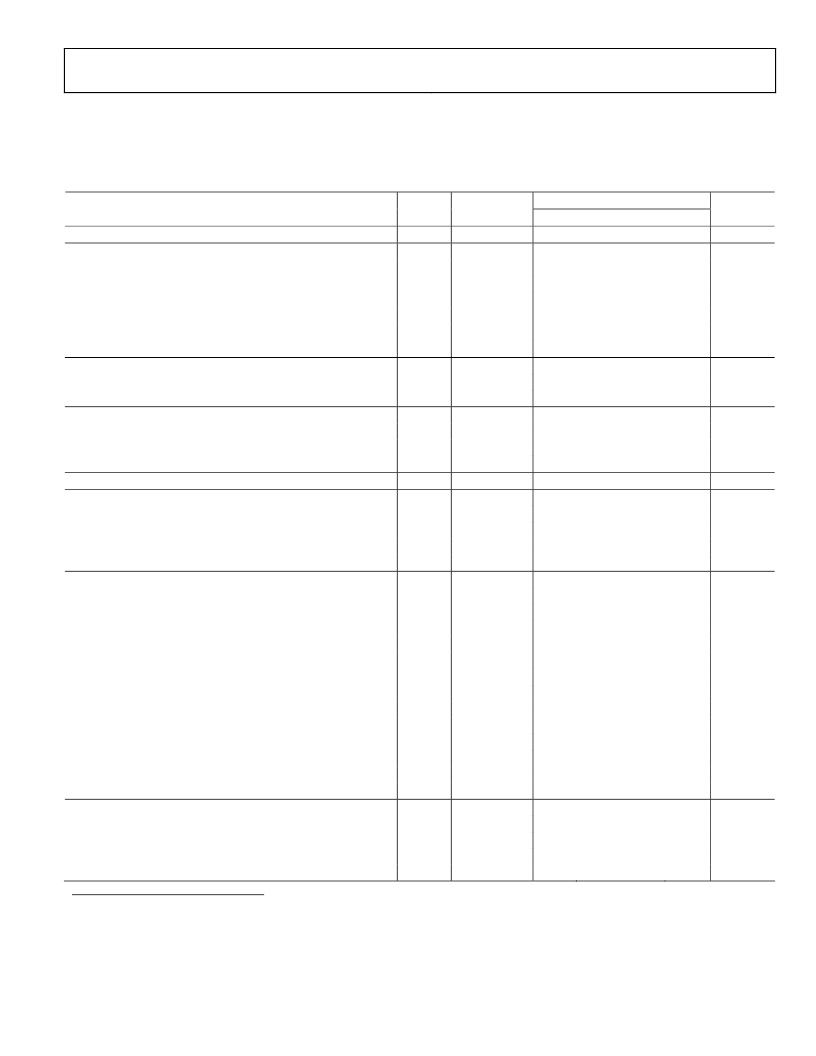
AD9444
DC SPECIFICATIONS
AVDD1 = 3.3 V, AVDD2 = 5.0 V, DRVDD = 3.3 V, LVDS mode, sample rate = 80 MSPS, 2 V p-p differential input, internal trimmed
reference (1.0 V mode), A
IN
= 0.5 dBFS, DCS on, unless otherwise noted.
Table 1.
Rev. 0 | Page 3 of 40
AD9444BSVZ-80
Typ
14
Guaranteed
±0.3
±0.4
±0.4
±0.6
12
0.002
1.0
±2
80
1.0
2
3.5
1
2.5
3.3
5.0
3.3
217
71
55
12
1
0.2
1.21
1.07
1.25
1.11
Parameter
RESOLUTION
ACCURACY
No Missing Codes
Offset Error
Gain Error
1
Differential Nonlinearity (DNL)
2
Integral Nonlinearity (INL)
2
TEMPERATURE DRIFT
Offset Error
Gain Error
VOLTAGE REFERENCE
Output Voltage
1
Load Regulation @ 1.0 mA
Reference Input Current (External 1.0 V Reference)
INPUT REFERRED NOISE
ANALOG INPUT
Input Span
Input Common-Mode Voltage
Input Resistance
3
Input Capacitance
3
POWER SUPPLIES
Supply Voltage
AVDD1
AVDD2
DRVDD—LVDS Outputs
DRVDD—CMOS Outputs
Supply Current
AVDD1
AVDD2
2
IDRVDD
2
—LVDS Outputs
IDRVDD
2
—CMOS Outputs
PSRR
Offset
Gain
POWER CONSUMPTION
DC Input—LVDS Outputs
DC Input—CMOS Outputs
Sine Wave Input
2
—LVDS Outputs
Sine Wave Input
2
—CMOS Outputs
Temp
Full
Full
Full
Full
Full
25°C
Full
Full
Full
Full
Full
Full
25°C
Full
Full
Full
Full
Full
Full
Full
Full
Full
Full
Full
Full
Full
Full
Full
Full
Full
Full
Test Level
VI
VI
VI
VI
VI
I
VI
V
V
VI
V
VI
V
V
V
V
V
IV
IV
IV
IV
VI
VI
VI
V
V
V
VI
V
VI
V
Min
6
3.0
0.8
1.3
1.7
0.87
3.14
4.75
3.0
3.0
Max
6
+3.0
+0.8
+1.3
+1.7
1.13
125
3.46
5.25
3.6
3.6
240
80
62
1.4
Unit
Bits
mV
% FSR
LSB
LSB
LSB
μV/°C
%FS/°C
V
mV
μA
LSB rms
V p-p
V
k
pF
V
V
V
V
mA
mA
mA
mA
mV/V
%/V
W
W
W
W
1
The internal voltage reference is trimmed at final test to minimize the gain error of the AD9444.
2
Measured at the maximum clock rate, f
IN
= 15 MHz, full-scale sine wave, with a 100 differential termination on each pair of output bits for LVDS output mode and
approximately 5 pF loading on each output bit for CMOS output mode.
3
Input capacitance or resistance refers to the effective impedance between one differential input pin and AGND. Refer to
structure.
for the equivalent analog input
Figure 6
相關(guān)PDF資料 |
PDF描述 |
|---|---|
| AD9444 | 14-Bit, 80 MSPS, A/D Converter |
| AD9445-IF-PCB | 14-Bit, 105/125 MSPS, IF Sampling ADC |
| AD9445BSVZ-105 | 14-Bit, 105/125 MSPS, IF Sampling ADC |
| AD9445BSVZ-125 | 14-Bit, 105/125 MSPS, IF Sampling ADC |
| AD9445 | 14-Bit, 105/125 MSPS, IF Sampling ADC |
相關(guān)代理商/技術(shù)參數(shù) |
參數(shù)描述 |
|---|---|
| AD9444-CMOS/PCB | 制造商:Analog Devices 功能描述:Evaluation Kit For 14-Bit, 80 MSPS, A/D Converter |
| AD9444-CMOSPCB | 制造商:AD 制造商全稱:Analog Devices 功能描述:High Speed ADC USB FIFO Evaluation Kit |
| AD9444-LVDS/PCB | 制造商:Analog Devices 功能描述:14-BIT, 80 MSPS ADC PB FREE EVAL BD. - Trays |
| AD9444-LVDS/PCBZ | 制造商:Analog Devices 功能描述:LVDS Mode Evaluation Board 制造商:Analog Devices 功能描述:14-BIT, 80 MSPS ADC EVAL BD. - Bulk |
| AD9444-LVDSPCB | 制造商:AD 制造商全稱:Analog Devices 功能描述:High Speed ADC USB FIFO Evaluation Kit |
發(fā)布緊急采購,3分鐘左右您將得到回復(fù)。