- 您現(xiàn)在的位置:買賣IC網(wǎng) > PDF目錄375243 > AD8315ARM (ANALOG DEVICES INC) 50 dB GSM PA Controller PDF資料下載
參數(shù)資料
| 型號(hào): | AD8315ARM |
| 廠商: | ANALOG DEVICES INC |
| 元件分類: | 通信及網(wǎng)絡(luò) |
| 英文描述: | 50 dB GSM PA Controller |
| 中文描述: | SPECIALTY TELECOM CIRCUIT, PDSO8 |
| 封裝: | MO-187AA, MSOP-8 |
| 文件頁數(shù): | 13/20頁 |
| 文件大?。?/td> | 1787K |
| 代理商: | AD8315ARM |
REV. B
AD8315
–13–
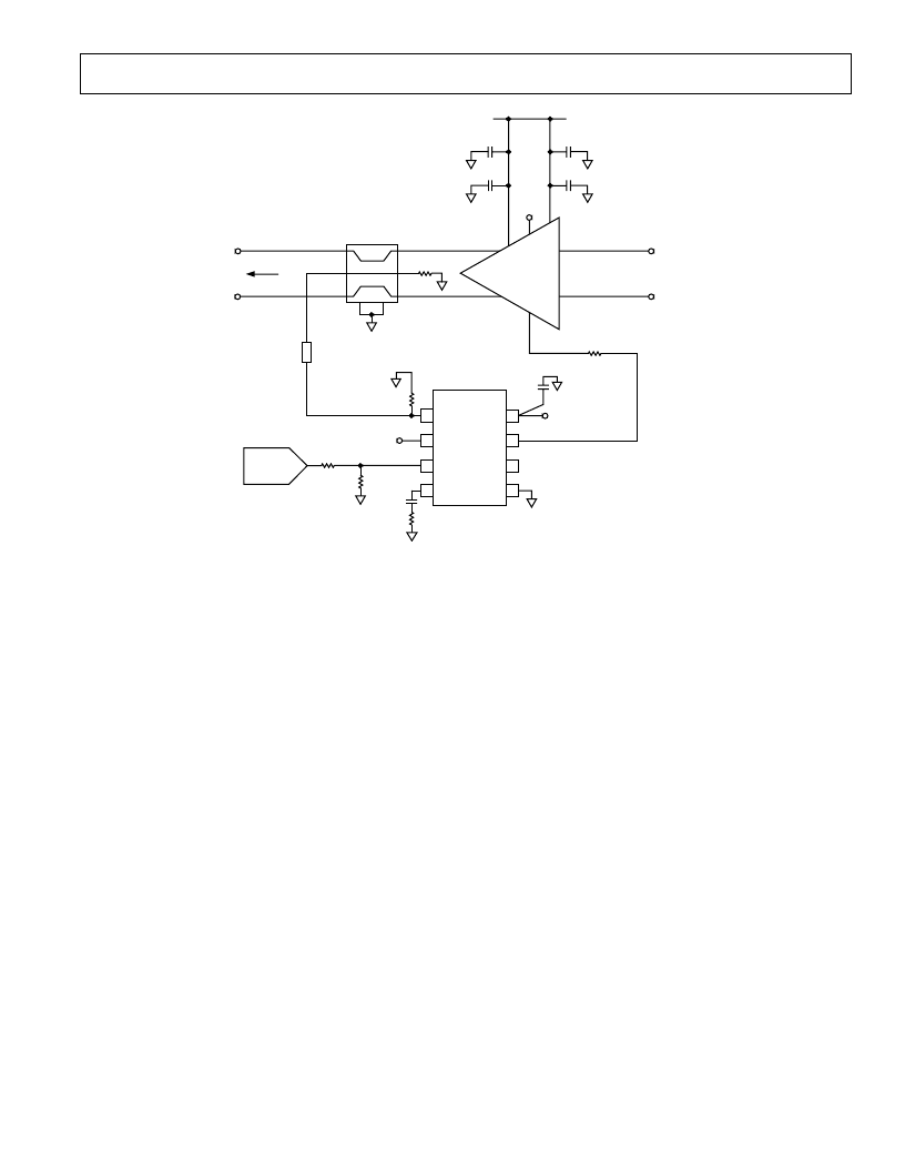
The PA has a single gain control line; the band to be used is
selected by applying either 0 V or 2 V to the PA’s VCTL input.
Some of the output power from the PA is coupled off using a
dual-band directional coupler (Murata part number
LDC15D190A0007A). This has a coupling factor of approxi-
mately 19 dB for the GSM band and 14 dB for DCS and an
insertion loss of 0.38 dB and 0.45 dB, respectively. Because the
PF08107B transmits a maximum power level of +35 dBm for
GSM and +32 dBm for DCS, additional attenuation of 20 dB is
required before the coupled signal is applied to the AD8315.
This results in peak input levels to the AD8315 of –4 dBm
(GSM) and –2 dBm (DCS). While the AD8315 gives a linear
response for input levels up to +2 dBm, for highly temperature-
stable performance at maximum PA output power, the maxi-
mum input level should be limited to approximately –2 dBm
(see TPC 3 and TPC 5). This does, however, reduce the sensi-
tivity of the circuit at the low end.
The operational setpoint voltage, in the range 250 mV to 1.4 V, is
applied to the VSET Pin of the AD8315. This will typically be
supplied by a digital-to-analog converter (DAC). The AD8315’s
VAPC output drives the level control pin of the power amplifier
directly. V
APC
reaches a maximum value of approximately 2.5 V
on a 2.7 V supply while delivering the 3 mA required by the level
control input of the PA. This is more than sufficient to exercise
the gain control range of the PA.
During initialization and completion of the transmit sequence,
VAPC should be held at its minimum level of 250 mV by keeping
VSET below 200 mV.
In this example, V
SET
is supplied by an 8-bit DAC that has an
output range from 0 V to 2.55 V or 10 mV per bit. This sets the
control resolution of VSET to 0.4 dB/bit (0.04 dB/mV times
10 mV). If finer resolution is required, the DAC’s output voltage
can be scaled using two resistors as shown. This converts the
DAC’s maximum voltage of 2.55 V down to 1.6 V and increases
the control resolution to 0.25 dB/bit.
A filter capacitor (C
FLT
) must be used to stabilize the loop. The
choice of C
FLT
will depend to a large degree on the gain control
dynamics of the power amplifier, something that is frequently
poorly characterized, so some trial and error may be necessary.
In this example, a 150 pF capacitor is used and a 1.5 k
W
series
resistor is included. This adds a zero to the control loop and
increases the phase margin, which helps to make the step response
of the circuit more stable when the PA output power is low and
the slope of the PA’s power control function is the steepest.
A smaller filter capacitor can be used by inserting a series
resistor between VAPC and the control input of the PA.
A series resistor will work with the input impedance of the
PA to create a resistor divider and will reduce the loop gain. The
size of the resistor divider ratio depends upon the available
output swing of V
APC
and the required control voltage on the PA.
This technique can also be used to limit the control voltage in
situations where the PA cannot deliver the power level being
demanded by VAPC. Overdrive of the control input of some
PAs causes increased distortion. It should be noted, however,
that if the control loop opens (i.e., VAPC goes to its maxi-
mum value in an effort to balance the loop), the quiescent current
of the AD8315 will increase somewhat, particularly at supply
voltages greater than 3 V.
NC = NO CONNECT
RFIN
ENBL
VSET
VPOS
VAPC
NC
COMM
FLTR
1
2
3
4
5
6
7
8
+V
S
2.7V
8-BIT
RAMP DAC
0V–2.55V
ENABLE
0V/2.7V
*
R2, R3 OPTIONAL,
*
SEE TEXT
BAND
SELECT
0V/2V
P
DCS
32dBm MAX
3
4
1
5
8
7
LDC15D190A0007A
2
6
ATTN
20dB
PF08107B
VCTL
VAPC
(OPTIONAL,
SEE TEXT)
P
GSM
3dBm
P
DCS
3dBm
TO
ANTENNA
1000pF
3.5V
1000pF
P
GSM
35dBm MAX
0.1 F
R3
*
1k
1.5k
150pF
R2
*
600
R1
52.3
49.9
4.7 F
4.7 F
500
AD8315
Figure 8. Dual Mode (GSM/DCS) PA Control Example
相關(guān)PDF資料 |
PDF描述 |
|---|---|
| AD8315ARM-REEL | 50 dB GSM PA Controller |
| AD8315ARM-REEL7 | 50 dB GSM PA Controller |
| AD831 | Low Distortion Mixer |
| AD831AP | Low Distortion Mixer |
| AD8320-EB | Serial Digital Controlled Variable Gain Line Driver |
相關(guān)代理商/技術(shù)參數(shù) |
參數(shù)描述 |
|---|---|
| AD8315ARM-REEL | 制造商:Rochester Electronics LLC 功能描述:- Tape and Reel |
| AD8315ARM-REEL7 | 制造商:Analog Devices 功能描述:50 DB GSM PA CONTROLLER - Tape and Reel 制造商:Rochester Electronics LLC 功能描述:50 DB GSM PA CONTROLLER - Tape and Reel |
| AD8315ARMZ | 功能描述:IC RF PA CTRLR 50DB GSM 8MSOP RoHS:是 類別:RF/IF 和 RFID >> RF 電源控制器 IC 系列:- 標(biāo)準(zhǔn)包裝:3,000 系列:- RF 型:GSM 頻率:450MHz ~ 2GHz 特點(diǎn):四頻帶 封裝/外殼:8-VFBGA 供應(yīng)商設(shè)備封裝:8-MicroSMD(1.51x1.51) 包裝:帶卷 (TR) 其它名稱:LMV243BLX |
| AD8315ARMZ-RL | 功能描述:IC RF PA CTRLR 50DB GSM 8MSOP RoHS:是 類別:RF/IF 和 RFID >> RF 電源控制器 IC 系列:- 標(biāo)準(zhǔn)包裝:3,000 系列:- RF 型:GSM 頻率:450MHz ~ 2GHz 特點(diǎn):四頻帶 封裝/外殼:8-VFBGA 供應(yīng)商設(shè)備封裝:8-MicroSMD(1.51x1.51) 包裝:帶卷 (TR) 其它名稱:LMV243BLX |
| AD8315CSURF | 制造商:AD 制造商全稱:Analog Devices 功能描述:50 dB GSM PA Controller |
發(fā)布緊急采購,3分鐘左右您將得到回復(fù)。