- 您現(xiàn)在的位置:買賣IC網(wǎng) > PDF目錄375243 > AD8303AR (ANALOG DEVICES INC) +3 V, Dual, Serial Input Complete 12-Bit DAC PDF資料下載
參數(shù)資料
| 型號(hào): | AD8303AR |
| 廠商: | ANALOG DEVICES INC |
| 元件分類: | DAC |
| 英文描述: | +3 V, Dual, Serial Input Complete 12-Bit DAC |
| 中文描述: | DUAL, SERIAL INPUT LOADING, 14 us SETTLING TIME, 12-BIT DAC, PDSO14 |
| 封裝: | 1.75 MM HEIGHT, SOIC-14 |
| 文件頁(yè)數(shù): | 11/16頁(yè) |
| 文件大?。?/td> | 414K |
| 代理商: | AD8303AR |
第1頁(yè)第2頁(yè)第3頁(yè)第4頁(yè)第5頁(yè)第6頁(yè)第7頁(yè)第8頁(yè)第9頁(yè)第10頁(yè)當(dāng)前第11頁(yè)第12頁(yè)第13頁(yè)第14頁(yè)第15頁(yè)第16頁(yè)
AD8303
REV. 0
–11–
SHUTDOWN (
SHDN
)
The shutdown feature is activated when
SHDN
is pulled low.
While the AD8303 is in shutdown mode, the voltage reference,
DACs, and output amplifiers are all turned off. Supply current
is less than 1
μ
A. The DAC output voltage goes to 0 V, pulled
to GND by the 12.5 k
feedback resistors (Figure 22).
If power (i.e., V
DD
) is maintained to the AD8303 during
shutdown, the value stored in the DAC input latches will not
change. When the
SHDN
pin is driven high, the DACs will
return to the same voltages as before shutdown. The CMOS
logic section of the AD8303 remains active while
SHDN
is low.
Thus, new data can be loaded while the DACs are shut down
and, when
SHDN
goes high, the DACs will assume the new
output voltage. The AD8303 recovers from shutdown very
quickly. The voltage output settling time after shutdown is
typically only a few microseconds longer than the normal
settling time (Figure 20).
SDI
CLK
CS
LDA
LDB
RS
MSB
SHDN
AD8303
13
2, 14
14
4
1
V
OUTA
V
OUTB
+3V TO +5V
AGND DGND
V
DD
500pF
2k
7
6
5
8
10
9
11
12
0.1μF
10μF
0V
≤
V
OUT
≤
2.0475V
V
OUTA
, V
OUTB
Figure 29. Unipolar Output Operation
UNIPOLAR OUTPUT OPERATION
This is the basic mode of operation for the AD8303. As shown
in Figure 29, the AD8303 has been designed to drive loads as
low as 2 k
in parallel with 500 pF. The code table for this
operation is shown in Table II.
Table II. Unipolar Code Table
Hexadecimal Number Decimal Number
in DAC Register
Analog Output
Voltage (V)
in DAC Register
FFF
801
800
7FF
000
4095
2049
2048
2047
0
2.0475
1.0245
1.024
1.0235
0
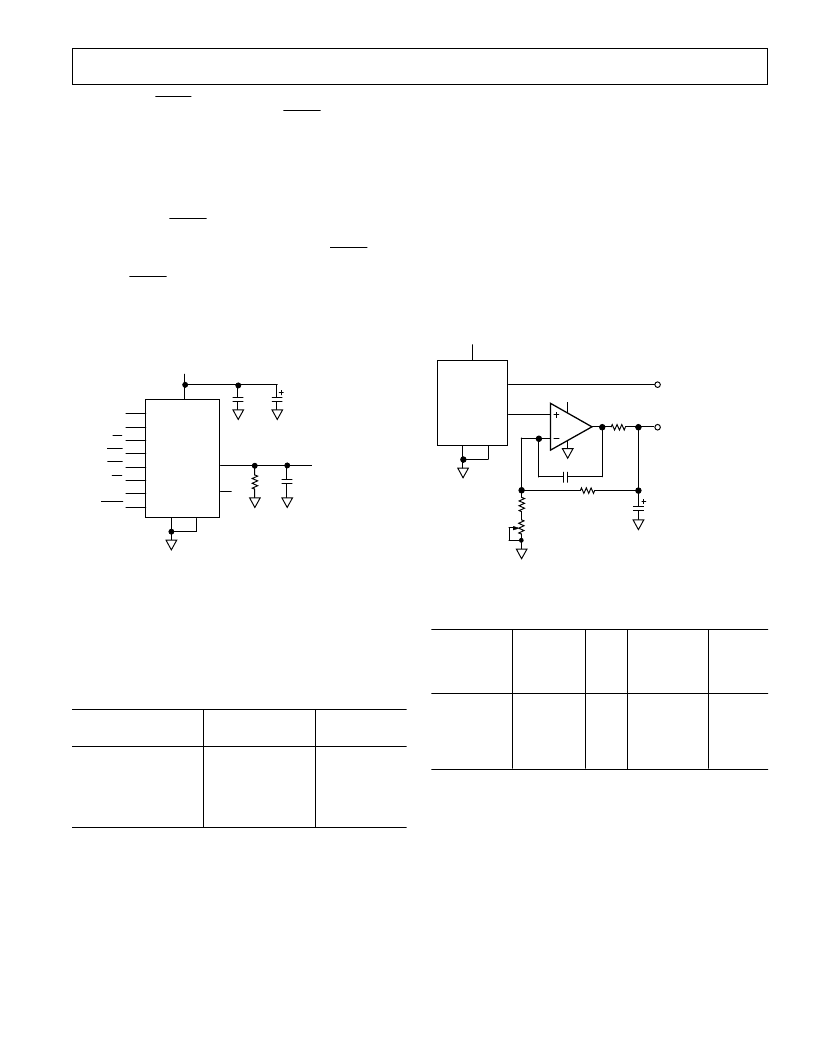
GENERATING “BIPOLAR” OUTPUTS WITH A SINGLE
SUPPLY
To maximize output signal swings in single supply operation,
many circuit designs employ a “false-ground” configuration.
This method defines a voltage, usually at one half of full scale or
at one half of the power supply, as the “ground” reference.
Signals are then measured differentially from the false ground,
which produces a “quasi-bipolar” output swing.
The AD8303’s voltage reference output, combined with an op
amp, can provide a temperature compensated false-ground
reference, as shown in Figure 30. The op amp amplifies the
AD8303’s 1.0 V reference by 1.024 to provide an analog
common (false ground) at one-half scale (1.024 V). With this
method, the DAC output is
±
1.024 V (referenced to the false
ground). The “Quasi-Bipolar” code table is given in Table III.
4
1
AD8303
13
2
3
V
OUTA
V
REF
+3V
AGND DGND
V
DD
+3V
OP193
V
=
±
1.024V
(REFERENCED TO
SIGNAL GROUND)
R2A
97.6k
1μF
0.022μF
R1
2.4k
SIGNAL GROUND
(FALSE GROUND, +1.024V)
100
R2B*
2k
*ZERO-SCALE TRIM
Figure 30. A False-Ground Generator
Table III. Quasi-Bipolar Code Table
DAC
Output
Voltage (False-Ground) Analog
Voltage (V)
Analog
Common
Hexadecimal
Number
in DAC Register DAC Register (V)
Decimal
Number In
“Bipolar”
Voltage (V)
FFF
801
800
7FF
000
4095
2049
2048
2047
0
2.0475
1.0245
1.024
1.0235
0
1.024
1.024
1.024
1.024
1.024
+1.2035
0.0005
0
–0.0005
–1.024
Since the AD8303’s reference voltage output limits are typical, a
trim potentiometer is included so that the “false-ground” output
can be adjusted to exactly 1.024 V. To maintain accuracy,
resistors R1 and R2A must be of the same type (preferably
metal film) to insure temperature coefficient matching. The
circuit includes compensation to allow for a 1
μ
F bypass
capacitor at the false-ground output. The benefit of a large
capacitor is that not only does the false ground present a very
low dc resistance to the load, but its ac impedance is low as
well.
相關(guān)PDF資料 |
PDF描述 |
|---|---|
| AD8309 | 5 MHz to 500 MHz 100 dB Demodulating Logarithmic Amplifier with Limiter Output(具有限幅輸出為的5MHz到500MHz,輸入動(dòng)態(tài)范圍為100dB的解調(diào)對(duì)數(shù)放大器) |
| AD8310 | Fast, Voltage-Out DC-440 MHz 95 dB Logarithmic Amplifier |
| AD8310-EVAL | Fast, Voltage-Out DC-440 MHz 95 dB Logarithmic Amplifier |
| AD8310ARM | Fast, Voltage-Out DC-440 MHz 95 dB Logarithmic Amplifier |
| AD8310ARM-REEL | Fast, Voltage-Out DC-440 MHz 95 dB Logarithmic Amplifier |
相關(guān)代理商/技術(shù)參數(shù) |
參數(shù)描述 |
|---|---|
| AD8303AR-REEL | 制造商:Analog Devices 功能描述:DAC 2-CH R-2R 12-bit 14-Pin SOIC N T/R 制造商:Rochester Electronics LLC 功能描述:IC,DUAL 12BIT,+3V,COMPLETE DAC,TAPE&REEL - Tape and Reel |
| AD8303ARZ-REEL | 功能描述:IC DAC 12BIT SERIAL 14SOIC RoHS:是 類別:集成電路 (IC) >> 數(shù)據(jù)采集 - 數(shù)模轉(zhuǎn)換器 系列:- 標(biāo)準(zhǔn)包裝:2,400 系列:- 設(shè)置時(shí)間:- 位數(shù):18 數(shù)據(jù)接口:串行 轉(zhuǎn)換器數(shù)目:3 電壓電源:模擬和數(shù)字 功率耗散(最大):- 工作溫度:-40°C ~ 85°C 安裝類型:表面貼裝 封裝/外殼:36-TFBGA 供應(yīng)商設(shè)備封裝:36-TFBGA 包裝:帶卷 (TR) 輸出數(shù)目和類型:* 采樣率(每秒):* |
| AD8303JRU | 制造商:Analog Devices 功能描述:DAC 2-CH R-2R 12-bit 14-Pin TSSOP 制造商:Rochester Electronics LLC 功能描述:IC,DUAL 12BIT,+3V,COMPLETE DAC - Bulk |
| AD8303JRU-REEL | 制造商:Analog Devices 功能描述:DAC 2-CH R-2R 12-bit 14-Pin TSSOP T/R |
| AD8303JRUZ | 制造商:Analog Devices 功能描述:DAC 2-CH R-2R 12-bit 14-Pin TSSOP |
發(fā)布緊急采購(gòu),3分鐘左右您將得到回復(fù)。