- 您現(xiàn)在的位置:買賣IC網(wǎng) > PDF目錄375243 > AD8200YCHIPS (ANALOG DEVICES INC) High Common-Mode Voltage, Single-Supply Difference Amplifier PDF資料下載
參數(shù)資料
| 型號: | AD8200YCHIPS |
| 廠商: | ANALOG DEVICES INC |
| 元件分類: | 運動控制電子 |
| 英文描述: | High Common-Mode Voltage, Single-Supply Difference Amplifier |
| 中文描述: | OP-AMP, 1000 uV OFFSET-MAX, UUC7 |
| 封裝: | DIE-7 |
| 文件頁數(shù): | 6/12頁 |
| 文件大?。?/td> | 231K |
| 代理商: | AD8200YCHIPS |
REV. B
–6–
AD8200
CURRENT SENSING
High Line, High Current Sensing
Basic automotive applications making use of the large common-
mode range are shown in Figures 1 and 2. The capability of the
device to operate as an amplifier in primary battery supply circuits
is shown in Figure 1; Figure 2 illustrates the ability of the device
to withstand voltages below system ground.
Low Current Sensing
The AD8200 can also be used in low current sensing applica-
tions, such as the 4–20 mA current loop shown in Figure 4. In
such applications, the relatively large shunt resistor can degrade
the common-mode rejection. Adding a resistor of equal value in
the low impedance side of the input corrects for this error.
5V
OUTPUT
10
10
1%
NC = NO CONNECT
1%
+
GND
NC
–IN
+IN
A1
+V
S
A2
OUT
AD8200
Figure 4. 4–20 mA Current Loop Receiver
GAIN ADJUSTMENT
The default gain of the preamplifier and buffer are 10 and 2,
respectively, resulting in a composite gain of 20. With the
addition of external resistor(s) or trimmer(s), the gain may be
lowered, raised, or finely calibrated.
Gains Less than 20
Since the preamplifier has an output resistance of 100 k
, an exter-
nal resistor connected from Pins 3 and 4 to GND will decrease the
gain by a factor R
EXT
/(100 k
+ R
EXT
) (see Figure 5).
10k
10k
100k
A2
A1
GND
–IN
OUT
+V
S
NC
+IN
AD8200
OUT
+V
S
R
EXT
V
CM
V
DIFF
GAIN =
20R
EXT
R
EXT
+ 100k
R
EXT
= 100k
GAIN
20 – GAIN
V
DIFF
NC = NO CONNECT
Figure 5. Adjusting for Gains Less than 20
The overall bandwidth is unaffected by changes in gain using
this method, although there may be a small offset voltage due to
the imbalance in source resistances at the input to the buffer. In
many cases this can be ignored, but if desired, can be nulled by
inserting a resistor equal to 100 k
minus the parallel sum of
R
EXT
and 100 k
, in series with Pin 4. For example, with R
EXT
= 100 k
(yielding a composite gain of 10), the optional offset
nulling resistor is 50 k
(see Figure 11.)
Gains Greater than 20
Connecting a resistor from the output of the buffer amplifier to
its noninverting input, as shown in Figure 6, will increase the
gain. The gain is now multiplied by the factor R
EXT
/(R
EXT
–
100 k
); for example, it is doubled for R
EXT
= 200 k
. Overall
gains as high as 50 are achievable in this way. Note that the
accuracy of the gain becomes critically dependent on resistor
value at high gains. Also, the effective input offset voltage at
Pins 1 and 8 (about six times the actual offset of A1) limits the
part’s use in very high gain, dc-coupled applications.
10k
10k
100k
A2
A1
–IN
+V
S
NC
+IN
AD8200
GND
OUT
OUT
+V
S
V
CM
GAIN =
20R
EXT
R
EXT
– 100k
R
EXT
= 100k
GAIN
GAIN – 20
R
EXT
V
DIFF
2
V
DIFF
NC = NO CONNECT
Figure 6. Adjusting for Gains Greater than 20
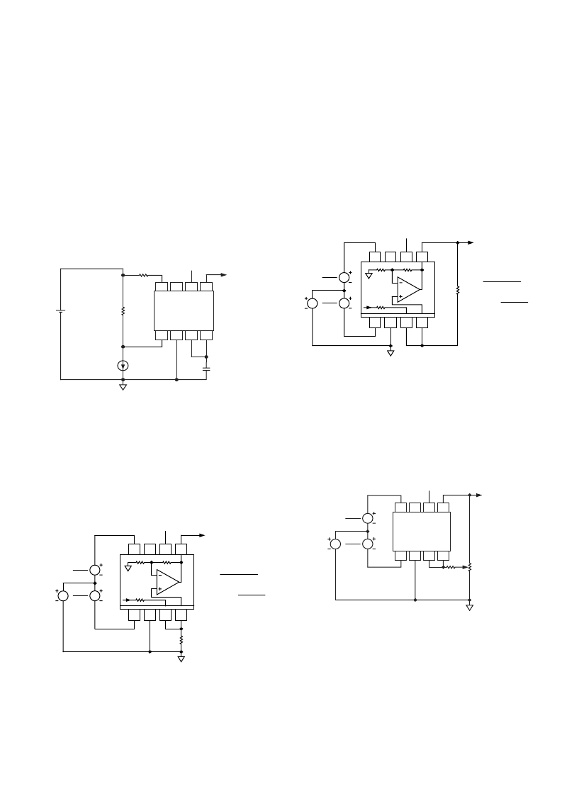
GAIN TRIM
Figure 7 shows a method for incremental gain trimming using a
trimpot and external resistor R
EXT
.
The following approximation is useful for small gain ranges
(
10
Thus, the adjustment range would be
±
2% for
R
EXT
= 5
M
;
±
10% for
R
EXT
= 1
M
, and so on.
G
M
R
EXT
≈
÷
)
%
5V
OUT
R
EXT
GAIN TRIM
20k
MIN
V
CM
V
DIFF
2
V
DIFF
2
NC = NO CONNECT
GND
NC
–IN
+IN
A1
+V
S
A2
OUT
AD8200
Figure 7. Incremental Gain Trim
相關(guān)PDF資料 |
PDF描述 |
|---|---|
| AD8200YCSURF | High Common-Mode Voltage, Single-Supply Difference Amplifier |
| AD8206YCSURF | Single-Supply 42 V System Difference Amplifier |
| AD8206YR | Single-Supply 42 V System Difference Amplifier |
| AD8206YR-REEL | Single-Supply 42 V System Difference Amplifier |
| AD8206YR-REEL7 | Single-Supply 42 V System Difference Amplifier |
相關(guān)代理商/技術(shù)參數(shù) |
參數(shù)描述 |
|---|---|
| AD8200YCSURF | 制造商:Analog Devices 功能描述: |
| AD8200YR | 制造商:Analog Devices 功能描述:AMP DIFF SINGLE SUPPLY SMD 8200 |
| AD8200YR-REEL | 制造商:Analog Devices 功能描述:SP Amp Difference Amplifier Dual 12V 8-Pin SOIC N T/R |
| AD8200YR-REEL7 | 制造商:Analog Devices 功能描述:SP Amp Difference Amplifier Dual 12V 8-Pin SOIC N T/R |
| AD8200YR-REEL-7 | 制造商:未知廠家 制造商全稱:未知廠家 功能描述:Amplifier. Other |
發(fā)布緊急采購,3分鐘左右您將得到回復(fù)。