- 您現(xiàn)在的位置:買賣IC網(wǎng) > PDF目錄375238 > AD7742 (Analog Devices, Inc.) Low Cost, Single & Multi-Channel,Voltage-to-Frequency Converters(低成本,多通道,電壓-頻率轉(zhuǎn)換器) PDF資料下載
參數(shù)資料
| 型號(hào): | AD7742 |
| 廠商: | Analog Devices, Inc. |
| 英文描述: | Low Cost, Single & Multi-Channel,Voltage-to-Frequency Converters(低成本,多通道,電壓-頻率轉(zhuǎn)換器) |
| 中文描述: | 低成本,單 |
| 文件頁(yè)數(shù): | 3/9頁(yè) |
| 文件大?。?/td> | 304K |
| 代理商: | AD7742 |
PRELMNARY
10
10
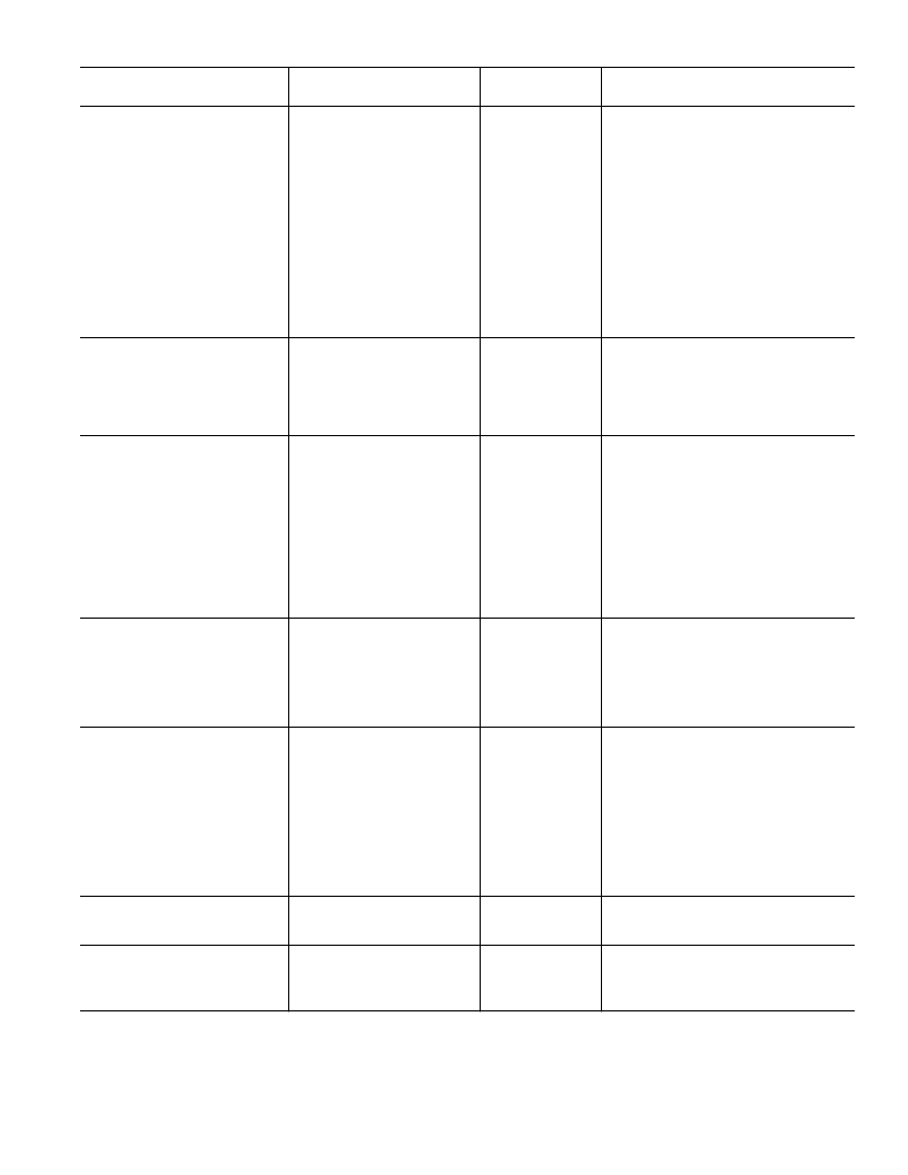
AD7742-PRELIMINARY SPECIFICATIONS
B
Versions
l
Y
Versions
1
Parameter
2
Units
Test Conditions/Comments
ACCURACY
Linearity Error
F
CLK
= 200 kHz
F
CLK
= 2 MHz
F
CLK
= 5 MHz
Channel-to-Channel Isolation
Power Supply Rejection Ratio
Unipolar Offset Error
Unipolar Offset Error Drift
Unipolar Gain Error
Unipolar Gain Error Drift
Bipolar Offset Error
Bipolar Zero Error
Bipolar Gain Error
CMR
±0.1
±0.1
±0.1
TBD
0.01
TBD
TBD
±0.5
TBD
±100
TBD
±0.5
TBD
±0.1
±0.1
±0.1
TBD
0.01
TBD
TBD
±0.5
TBD
±100
TBD
±0.5
TBD
% of Span max.
% of Span max.
% of Span max.
dB typ
%/V max
μ
V max.
μ
V/°C typ.
% of Span max.
ppm/°C typ.
μ
V max.
μ
V max.
% of Span max.
dB
V
IN
=kHz
ANALOG INPUT
Input Current
Common Mode Range
4
±1.0
-300mV to
±REF/Gain
0 to REF/Gain 0 to REF/Gain
±1.0
-300mV to
±REF/Gain
nA typ
100nA max.
Volts
Volts
Differential Input Voltage Range
Unipolar Input Range
VOLTAGE REFERENCE
REF IN
Input Voltage
Input Impedance
REF OUT
Output Voltage Accuracy
Output Temp Coeff
Line Regulation
Load Regulation
Noise (0.1 Hz - 10 Hz)
Output Resistance
Output Capacitance
2.5
TBD
2.5
TBD
V nom
k
typ
2.4/2.6
100
TBD
TBD
TBD
100
TBD
2.4/2.6
100
TBD
TBD
TBD
100
TBD
V min/V max
ppm/°C typ
μV/V max
μV/mA max
μV (p-p) typ
k
typ
pF typ
LOGIC OUTPUT (F
OUT
)
Output High Voltage, V
INH
Output Low Voltage, V
INL
Output Frequency
4.0
0.4
0.05F
CLOCK
4.0
0.4
0.05F
CLOCK
V min
V max
kHz min
I
SOURCE
= 800
μ
A except for CLK
OUT
I
SINK
= 1.6 mA except for CLK
OUT
V
IN
=0V (Unipolar)
V
IN
=-REF IN/Gain (Bipolar)
V
IN
=+REF IN/Gain (Unipolar)
V
IN
=+REF IN/Gain (Bipolar)
0.45F
CLOCK
0.45F
CLOCK
kHz max
LOGIC INPUTS
3
ALL INPUTS EXCEPT CLK
IN
Input High Voltage, V
INH
Input Low Voltage, V
INL
Input Current, I
IN
Input Capacitance, C
IN
CLK
IN
ONLY
Input High Voltage, V
INH
Input Low Voltage, V
INL
Input Current, I
IN
Input Capacitance, C
IN
CLOCK FREQUENCY
F
CLKIN
2.0
0.8
2.0
0.8
V min
V max
μA max
pF typ
V
DD
= 5 V ± 5%
V
DD
= 5 V ± 5%
V
IN
= 0 V to V
DD
3.5
0.8
±10
10
3.5
0.8
±10
10
V min
V max
μA max
pF typ
V
DD
= 5 V ± 5%
V
DD
= 5 V ± 5%
V
IN
= 0 V to V
DD
100
5
100
5
kHz min
MHz max
For Specified performance
POWER REQUIREMENTS
V
DD
I
DD
Power Dissipation
+5
8
40
+5
8
40
V nom
mA max
mW max
±5% for Specified Performance
V
DD
= 5V± 5%
Typically 30mW
NOTES
1
Temperature Ranges are as follows: B Version, 40°C to +85°C; Y Version, 40°C to +105°C.
2
See Terminology.
3
Guaranteed by design and characterization, not production tested.
4
The absolute input voltage on the different input pins must not go more positive than Vdd - 2V or more negative than GND - 400mV. The common-mode voltage
applies to those inputs which form differential pairs.
Span = Max output frequency - Min output frequency
Specifications subject to change without notice.
(V
DD
= +5 V ± 5%, External Reference =
+2.5 V; F
CLK
= 5MHz; All specifications T
MIN
to
T
MAX
unless otherwise noted.)
PRELIM. J1 7/98
3
相關(guān)PDF資料 |
PDF描述 |
|---|---|
| AD7746ARUZ-REEL | 24-Bit Capacitance-to-Digital Converter with Temperature Sensor |
| AD7745 | 24-Bit Capacitance-to-Digital Converter with Temperature Sensor |
| AD7745ARUZ | 24-Bit Capacitance-to-Digital Converter with Temperature Sensor |
| AD7745ARUZ-REEL | 24-Bit Capacitance-to-Digital Converter with Temperature Sensor |
| AD7745ARUZ-REEL7 | 24-Bit Capacitance-to-Digital Converter with Temperature Sensor |
相關(guān)代理商/技術(shù)參數(shù) |
參數(shù)描述 |
|---|---|
| AD7742BN | 制造商:Analog Devices 功能描述:VFC Sync 2.75MHz 16-Pin PDIP 制造商:Rochester Electronics LLC 功能描述:SINGLE + MULTI-CHANNEL VFC I.C. - Bulk |
| AD7742BNZ | 制造商:Analog Devices 功能描述:VFC Sync 2.75MHz 16-Pin PDIP |
| AD7742BR | 制造商:AD 制造商全稱:Analog Devices 功能描述:Single and Multichannel, Synchronous Voltage-to-Frequency Converters |
| AD7742BR-REEL | 制造商:Analog Devices 功能描述: |
| AD7742YR | 制造商:AD 制造商全稱:Analog Devices 功能描述:Single and Multichannel, Synchronous Voltage-to-Frequency Converters |
發(fā)布緊急采購(gòu),3分鐘左右您將得到回復(fù)。