- 您現(xiàn)在的位置:買賣IC網(wǎng) > PDF目錄375233 > AD5539 (Analog Devices, Inc.) Ultrahigh Frequency Operational Amplifier(超高頻率運算放大器) PDF資料下載
參數(shù)資料
| 型號: | AD5539 |
| 廠商: | Analog Devices, Inc. |
| 英文描述: | Ultrahigh Frequency Operational Amplifier(超高頻率運算放大器) |
| 中文描述: | 超高頻率運算放大器(超高頻率運算放大器) |
| 文件頁數(shù): | 14/16頁 |
| 文件大小: | 499K |
| 代理商: | AD5539 |
AD5539
REV. B
–14–
Figure 43. A Simulated Ideal Test Circuit Error Signal
Hence, the gain is unity at V
X
= +2 V. Since V
X
can overrange
to +3.3 V, the maximum gain in this configuration is about
4.3 dB. (Note: If Pin 9 of the AD539 is grounded, rather than
connected to the output of the 5539N, the maximum gain be-
comes 10 dB.)
T he bandwidth of this circuit is over 50 MHz at full gain, and is
not substantially affected at lower gains. Of course, when V
X
is
zero (or slightly negative, to override the residual input offset)
there is still a small amount of capacitive feedthrough at high
frequencies; therefore, extreme care is needed in laying out the
PC board to minimize this effect. Also, for small values of V
X
,
the combination of this feedthrough with the multiplier output
can cause a dip in the response where they are out of phase.
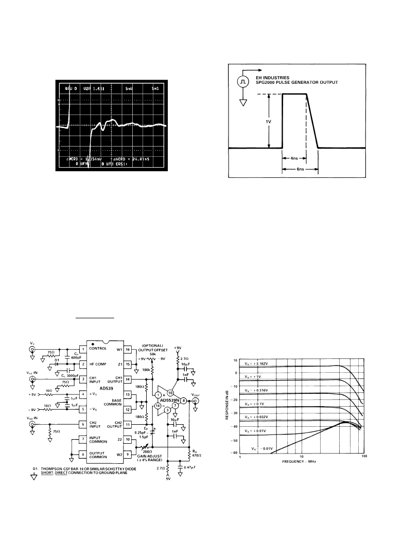
Figure 45 shows the ac response from the noninverting input,
with the response from the inverting input, V
Y2
, essentially iden-
tical. T est conditions: V
Y1
= 0.5 V rms for values of V
X
from
+10 mV to +3.16 V; this is with a 75
load on the output. T he
feedthrough at V
X
= –10 mV is also shown.
Figure 45. AC Response of the VCA at Different Gains
V
Y
= 0.5 V RMS
Figure 42 shows the oscilloscope response of the generator
alone, set up to simulate the ideal test circuit error signal
(Figure 43).
Figure 42. The Oscilloscope Response Alone Directly
Driven by the Test Generator. Vertical Scale: 5 ns/div.;
Horizontal Scale: 500
μ
V/div
A 50 MHz VOLT AGE -CONT ROLLE D AMPLIFIE R
Figure 44 is a circuit for a 50 MHz voltage-controlled amplifier
(VCA) suitable for use in high quality video-speed applications.
T his circuit uses the AD5539 as an output amplifier for the
AD539, a high bandwidth multiplier. T he outputs from the two
signal channels of the AD539 are applied to the op amp in a
subtracting configuration. T his connection has two main advan-
tages: first, it results in better rejection of the control voltage,
particularly when over-driven (V
X
< 0 or V
X
> 3.3 V). Secondly,
it provides a choice of either noninverting or inverting responses,
using either input V
Y1
or V
Y2
, respectively. In this circuit, the
output of the op amp will equal:
V
OUT
=
V
X
V
Y
1±
V
Y
2
(
2
V
)
for V
X
> 0
Figure 44. A Wide Bandwidth Voltage-Controlled Amplifier
相關PDF資料 |
PDF描述 |
|---|---|
| AD5547 | Dual Current Output, Parallel Input, 16-/14-Bit Multiplying DACs with 4-Quadrant Resistors |
| AD5547BRU | Dual Current Output, Parallel Input, 16-/14-Bit Multiplying DACs with 4-Quadrant Resistors |
| AD5547BRU-REEL7 | Dual Current Output, Parallel Input, 16-/14-Bit Multiplying DACs with 4-Quadrant Resistors |
| AD5557 | Dual Current Output, Parallel Input, 16-/14-Bit Multiplying DACs with 4-Quadrant Resistors |
| AD5557CRU | Dual Current Output, Parallel Input, 16-/14-Bit Multiplying DACs with 4-Quadrant Resistors |
相關代理商/技術參數(shù) |
參數(shù)描述 |
|---|---|
| AD5539J | 制造商:AD 制造商全稱:Analog Devices 功能描述:Ultrahigh Frequency Operational Amplifier |
| AD5539JN | 制造商:未知廠家 制造商全稱:未知廠家 功能描述:Voltage-Feedback Operational Amplifier |
| AD5539JQ | 制造商:Rochester Electronics LLC 功能描述:- Bulk |
| AD5539S | 制造商:AD 制造商全稱:Analog Devices 功能描述:Ultrahigh Frequency Operational Amplifier |
| AD5539SQ | 制造商:AD 制造商全稱:Analog Devices 功能描述:Ultrahigh Frequency Operational Amplifier |
發(fā)布緊急采購,3分鐘左右您將得到回復。