- 您現(xiàn)在的位置:買賣IC網(wǎng) > PDF目錄375232 > AD5260 (Analog Devices, Inc.) 4-Channel Digital Potentiometers(???é??é????°?-???μ?????¨) PDF資料下載
參數(shù)資料
| 型號: | AD5260 |
| 廠商: | Analog Devices, Inc. |
| 元件分類: | 通用總線功能 |
| 英文描述: | 4-Channel Digital Potentiometers(???é??é????°?-???μ?????¨) |
| 中文描述: | 4通道數(shù)字電位器(四通道數(shù)字電位器) |
| 文件頁數(shù): | 7/20頁 |
| 文件大小: | 853K |
| 代理商: | AD5260 |
REV. 0
–7–
AD5260/AD5262
THEORY OF OPERATION
The AD5260/AD5262 provide a single- or dual-channel, 256-position
digitally controlled variable resistor (VR) device and operate up to
15 V maximum voltage. Changing the programmed VR settings
is accomplished by clocking an 8-/9-bit serial data word into the
SDI (Serial Data Input) pin. For the AD5262, the format of this
data word is one address bit. A0 represents the first bit B8, then
followed by eight data bits B7–B0 with MSB first. Tables I and II
provide the serial register data word format. See Table III for the
AD5262 address assignment to decode the location of the VR latch
receiving the serial register data in bits B7 through B0. VR outputs
can be changed one at a time in random sequence. The AD5260/
AD5262 presets to a mid-scale, simplifying fault condition recov-
ery at power-up. Mid-scale can also be achieved at any time by
asserting the
PR
pin. Both parts have an internal power ON preset
that places the wiper in a mid-scale preset condition at power ON.
Operation of the power ON preset function depends only on the
state of the V
L
pin.
The AD5260/AD5262 contains a power shutdown
SHDN
pin,
which places the RDAC in an almost zero power consumption
state where terminals Ax are open circuited, and the wiper W is con-
nected to B, resulting in only leakage currents being consumed in
the VR structure. In the shutdown mode, the VR latch settings are
maintained so that, returning to operational mode from power
shutdown, the VR settings return to their previous resistance values.
Table III. AD5262 Address Decode Table
A0
Latch Loaded
0
1
RDAC#1
RDAC#2
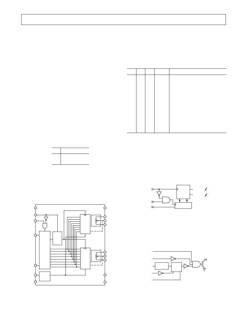
DIGITAL INTERFACING
The AD5260/AD5262 contains a 4-wire SPI-compatible
digital interface (SDI, SDO,
CS
, and CLK). For the AD5260,
the 8-bit serial word must be loaded with MSB first, and the
format of the word is shown in Table I. For the AD5262, the
9-bit serial word must be loaded with address bit A0 first, then
MSB of the data. The format of the word is shown in Table II.
A0
SER
REG
D7
D6
D5
D4
D3
D2
D1
D0
A1
W1
B1
V
DD
CS
CLK
SDO
A2
W2
B2
GND
RDAC
LATCH
#1
RDAC
LATCH
#2
PR
V
SS
PR
SDI
V
L
SHDN
POWER-
ON
PRESET
EN
ADDR
DEC
PR
Figure 3. AD5262 Block Diagram
The positive-edge sensitive CLK input requires clean transitions
to avoid clocking incorrect data into the serial input register.
Standard logic families work well. If mechanical switches are used
for product evaluation, they should be debounced by a flip-flop or
other suitable means. Figure 3 shows more detail of the internal
digital circuitry. When
CS
is low, the clock loads data into the
serial register on each positive clock edge (see Table IV).
Table IV. Truth Table
CLK
CS
PR
SHDN
Register Activity
L
≠
*
L
L
H
H
H
H
No SR effect, enables SDO pin
Shift one bit in from the SDI pin.
The eighth previously entered bit is
shifted out of the SDO pin.
Load SR data into RDAC latch
No Operation
Sets all RDAC latches to Mid-Scale,
wiper centered, and SDO latch
cleared.
Latches all RDAC latches to 80
H
.
Open circuits all resistor A–terminals,
connects W to B, turns off SDO
output transistor.
X
X
X
≠
H
X
H
H
L
H
H
H
X
X
H
H
≠
H
H
L
*
≠
= positive edge, X = don’t care, SR = shift register
The data setup and data hold times in the specification table
determine the data valid time requirements. The AD5260 uses
an 8-bit serial input data register word that is transferred to the
internal RDAC register when the
CS
line returns to logic high.
For the AD5262 the last 9 bits of the data word entered into the
serial register are held when
CS
returns high. Any extra bits are
ignored. At the same time
CS
goes high, it gates the address
decoder enabling AD5262 one of two positive edge-triggered
AD5262 RDAC latches (see Figure 4).
RDAC 1
RDAC 2
AD5260/AD5262
SDI
CLK
CS
ADDR
DECODE
SERIAL
REGISTER
Figure 4. Equivalent Input Control Logic
The target RDAC latch is loaded with the last 8 bits of the serial data
word completing one RDAC update. For the AD5262, two separate
9-bit data words must be clocked in to change both VR settings.
During shutdown (
SHDN
) the SDO output pin is forced to the
off (logic high state) to disable power dissipation in the pull-up
resistor. See Figure 5 for equivalent SDO output circuit schematic.
SDI
CLK
CS
SHDN
PR
SERIAL
REGISTER
D
Q
CK
RS
SDO
Figure 5. Detail SDO Output Schematic of the AD5260
相關(guān)PDF資料 |
PDF描述 |
|---|---|
| AD526 | Software Programmable Gain Amplifier(軟件可編程增益放大器) |
| AD5290 | Compact +30V/【15V 256-Position Digital Potentiometer |
| AD5290EVAL | Compact +30V/【15V 256-Position Digital Potentiometer |
| AD5290YRMZ10 | Compact +30V/【15V 256-Position Digital Potentiometer |
| AD5290YRMZ100 | Compact +30V/【15V 256-Position Digital Potentiometer |
相關(guān)代理商/技術(shù)參數(shù) |
參數(shù)描述 |
|---|---|
| AD5260_10 | 制造商:AD 制造商全稱:Analog Devices 功能描述:1-/2-Channel 15 V Digital Potentiometer |
| AD5260BRU20 | 制造商:Analog Devices 功能描述:Digital Potentiometer 256POS 20KOhm Single 14-Pin TSSOP 制造商:Analog Devices 功能描述:IC DIGITAL POTENTIOMETER 8-BIT |
| AD5260BRU200 | 制造商:Analog Devices 功能描述:Digital Potentiometer 256POS 200KOhm Single 14-Pin TSSOP 制造商:Analog Devices 功能描述:IC DIGITAL POTENTIOMETER 8-BIT |
| AD5260BRU200-REEL7 | 制造商:Analog Devices 功能描述:Digital Potentiometer 256POS 200KOhm Single 14-Pin TSSOP T/R 制造商:Rochester Electronics LLC 功能描述:8-BIT SPI DIG POT - Tape and Reel |
| AD5260BRU20-REEL7 | 制造商:Analog Devices 功能描述:Digital Potentiometer 256POS 20KOhm Single 14-Pin TSSOP T/R |
發(fā)布緊急采購,3分鐘左右您將得到回復(fù)。