- 您現(xiàn)在的位置:買賣IC網(wǎng) > PDF目錄375225 > AC08DSMA (NEC Corp.) ECONOLINE: RB & RA - Dual Output from a Single Input Rail- Power Sharing on Output- Industry Standard Pinout- 1kVDC & 2kVDC Isolation- Custom Solutions Available- UL94V-0 Package Material- Efficiency to 85% PDF資料下載
參數(shù)資料
| 型號(hào): | AC08DSMA |
| 廠商: | NEC Corp. |
| 英文描述: | ECONOLINE: RB & RA - Dual Output from a Single Input Rail- Power Sharing on Output- Industry Standard Pinout- 1kVDC & 2kVDC Isolation- Custom Solutions Available- UL94V-0 Package Material- Efficiency to 85% |
| 中文描述: | 8A條樹脂絕緣型可控硅 |
| 文件頁數(shù): | 2/6頁 |
| 文件大?。?/td> | 144K |
| 代理商: | AC08DSMA |
Data Sheet D10613EJ5V0DS
2
AC08DSMA,AC08FSMA
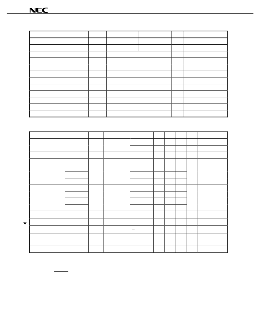
MAXIMUM RATINGS
Parameter
Symbol
AC08DSMA
AC08FSMA
Unit
Remarks
Non-repetitive Peak Off-state Voltage
V
DSM
500
700
V
Repetitive Peak Off-state Voltage
V
DRM
400
600
V
Effective On-state Current
I
T(RMS)
8 (T
C
= 88°C)
A
Refer to
Figure 11
and
12
.
Surge On-state Current
I
TSM
A
Refer to
Figure 2
.
80 (50 Hz 1 cycle)
88 (60 Hz 1 cycle)
Fusing Current
∫
i
T2
dt
28 (1 ms
≤
t
≤
10 ms)
A
2
s
Critical Rate Rise of On-state Current
dI
T
/dt
50
A/
μ
s
Peak Gate Power Dissipation
P
GM
5.0 (f
≥
50 Hz, Duty
≤
10%)
W
Average Gate Power Dissipation
P
G(AV)
0.5
W
Peak Gate Current
I
GM
±3 (f
≥
50 Hz, Duty
≤
10%)
A
Junction Temperature
T
j
40
~
+125
°
C
Storage Temperature
T
stg
55
~
+150
°
C
ELECTRICAL CHARACTERISTICS (T
j
= 25
°
C)
Parameter
Symbol
Conditions
MIN.
TYP. MAX.
Unit
Remarks
Repetitive Peak Off-state Current
I
DRM
V
DM
= V
DRM
T
j
= 25°C
100
μ
A
T
j
= 125°C
2
mA
On-state Voltage
V
TM
I
TM
= 10 A
1.6
V
Refer to
Figure 1
.
Gate Trigger Current
Mode I
I
GT
V
DM
= 12 V,
T
2
+, G+
20
mA Refer to
Figure 4
.
II
R
L
= 30
T
2
, G+
III
T
2
, G
20
IV
T
2
+, G
20
Gate Trigger Voltage
Mode I
V
GT
V
DM
= 12 V,
T
2
+, G+
1.5
V
Refer to
Figure 4
.
II
R
L
= 30
T
2
, G+
III
T
2
, G
1.5
IV
T
2
+, G
1
V
DRM
1.5
Gate Non-trigger Voltage
V
GD
T
j
= 125°C, V
DM
=
2
0.3
V
Holding Current
I
H
V
DM
= 24 V, I
TM
= 10 A
30
mA
Critical Rate Rise of Off-state Voltage
dv/dt
T
j
= 125°C, V
DM
=
3
2
V
DRM
100
V
/μ
s
Commutating Critical Rate Rise of
Off-state Voltage
Thermal Resistance
Note
(dv/dt)c T
j
= 125°C,
(di
T
/dt)c =
4 A/ms, V
D
= 400
V
10
V
/μ
s
R
th(j-c)
Junction-to-case AC
3.7
°C/W Refer to
Figure 13
.
Note
The thermal resistance with a 50 Hz or 60 Hz sine wave current, as shown in the following expression:
R
th(j-c)
=
)
AV
(
T
C
(max)
P
j
T
T
T
j(max)
: Maximum junction temperature
T
C
: Case temperature
P
T(AV)
: Average on-dissipation
相關(guān)PDF資料 |
PDF描述 |
|---|---|
| AC0V8DGM | 0.8 A MOLD TRIAC |
| AC10DGM | 10A MOLD TRIAC |
| AC10EGM | 10A MOLD TRIAC |
| AC10FGM | 10A MOLD TRIAC |
| AC10DSMA | 10 A RESIN INSULATION TYPE TRIAC |
相關(guān)代理商/技術(shù)參數(shù) |
參數(shù)描述 |
|---|---|
| AC08DSMA(AZ) | 制造商:Renesas Electronics Corporation 功能描述: |
| AC08E14S-5S(003) | 制造商:Amphenol Aerospace 功能描述: |
| AC08EGM | 制造商:TECCOR 制造商全稱:TECCOR 功能描述:Thyristor Product Catalog |
| AC08ESM | 制造商:TECCOR 制造商全稱:TECCOR 功能描述:Thyristor Product Catalog |
| AC08FGM | 制造商:TECCOR 制造商全稱:TECCOR 功能描述:Thyristor Product Catalog |
發(fā)布緊急采購,3分鐘左右您將得到回復(fù)。