- 您現(xiàn)在的位置:買賣IC網(wǎng) > PDF目錄375142 > A49LF004TL-33C (AMIC Technology Corporation) 4 Mbit CMOS 3.3Volt-only Firmware Hub Flash Memory PDF資料下載
參數(shù)資料
| 型號(hào): | A49LF004TL-33C |
| 廠商: | AMIC Technology Corporation |
| 英文描述: | 4 Mbit CMOS 3.3Volt-only Firmware Hub Flash Memory |
| 中文描述: | 4兆位的CMOS 3.3Volt只閃存固件集線器 |
| 文件頁數(shù): | 5/32頁 |
| 文件大小: | 595K |
| 代理商: | A49LF004TL-33C |
第1頁第2頁第3頁第4頁當(dāng)前第5頁第6頁第7頁第8頁第9頁第10頁第11頁第12頁第13頁第14頁第15頁第16頁第17頁第18頁第19頁第20頁第21頁第22頁第23頁第24頁第25頁第26頁第27頁第28頁第29頁第30頁第31頁第32頁
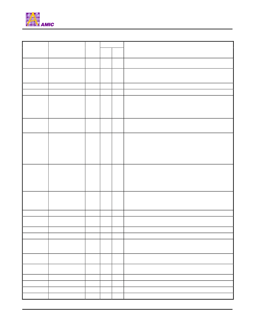
Table 1: Pin Description
A49LF004
PRELIMINARY (November, 2003, Version 0.0)
4
AMIC Technology, Corp.
1. IN=Input, OUT=output, I/O=Input/Output, PWR=Power
Interface
A/A
Mux
Symbol
Pin Name
Type
FWH
Descriptions
A
10
-A
0
Address
IN
X
Inputs for addresses during Read and Write operations in A/A
Mux mode. Row and column addresses are latched by R/C# pin.
I/O
7
-I/O
0
Data
I/O
X
To output data during Read cycle and receive input data during
Write cycle in A/A Mux mode. The outputs are in tri-state when
OE# is high.
OE#
Output Enable
IN
X
To control the data output buffers.
WE#
Write Enable
IN
X
To control the Write operations.
IC
Interface
Configuration Pin
IN
X
X
To determine which interface is operational. When held high, A/A
Mux mode is enabled and when held low, FWH mode is enabled.
This pin must be setup at power-up or before return from reset
and not change during device operation. This pin is internally
pulled down with a resistor between 20-100 K
.
INIT#
Initialize
IN
X
This is the second reset pin for in-system use. INIT# and RST#
pins are internally combined and initialize a device reset when
driven low.
ID[3:0]
Identification Inputs
IN
X
These four pins are part of the mechanism that allows multiple
FWH devices to be attached to the same bus. To identify the
component, the correct strapping of these pins must be set. The
boot device must have ID[3:0]=0000 and it is recommended that
all subsequent devices should use sequential up-count
strapping. These pins are internally pulled down with a resistor
between 20-100 K
.
FGPI[4:0]
General Purpose
Inputs
IN
X
These individual inputs can be used for additional board
flexibility. The state of these pins can be read immediately at
boot, through FWH internal registers. These inputs should be at
their desired state before the start of the PCI clock cycle during
which the read is attempted, and should remain in place until the
end of the Read cycle. Unused FGPI pins must not be floated.
TBL#
Top Block Lock
IN
X
To prevent any write operations to the Boot Block when driven
low, regardless of the state of the block lock registers. When
TBL# is high it disables hardware write protection for the top
Boot Block. This pin cannot be left unconnected.
FWH[3:0]
FWH I/Os
I/O
X
I/O Communications in FWH mode.
CLK
Clock
IN
X
To provide a clock input to the device. This pin is the same as
that for the PCI clock and adheres to the PCI specifications.
FWH4
FWH Input
IN
X
Input communication in FWH mode.
RST#
Reset
IN
X
X
To reset the operation of the device
WP#
Write Protect
IN
X
When low, prevents any write operations to all but the highest
addressable block. When WP# is high it disables hardware write
protection for these blocks. This pin cannot be left unconnected.
R/C#
Row/Column Select
IN
X
This pin determines whether the address pins are pointing to the
row addresses or the column addresses in A/A Mux mode.
RB#
Ready/Busy#
OUT
X
To determine if the device is busy in write operations. Valid only
in A/A Mux mode.
RES
Reserved
X
Reserved. These pins must be left unconnected.
VDD
Power Supply
PWR
X
X
To provide power supply (3.0-3.6Volt).
VSS
Ground
PWR
X
X
Circuit ground. All VSS pins must be grounded.
NC
No Connection
X
X
Unconnected pins.
相關(guān)PDF資料 |
PDF描述 |
|---|---|
| A49LF004 | 4 Mbit CMOS 3.3Volt-only Firmware Hub Flash Memory |
| A49LF040A | 4 Mbit CMOS 3.3Volt-only Low Pin Count Flash Memory |
| A49LF040ATL-33 | 4 Mbit CMOS 3.3Volt-only Low Pin Count Flash Memory |
| A49LF040ATL-33F | 4 Mbit CMOS 3.3Volt-only Low Pin Count Flash Memory |
| A49LF040ATX-33 | 4 Mbit CMOS 3.3Volt-only Low Pin Count Flash Memory |
相關(guān)代理商/技術(shù)參數(shù) |
參數(shù)描述 |
|---|---|
| A49LF004TX-33C | 制造商:AMICC 制造商全稱:AMIC Technology 功能描述:4 Mbit CMOS 3.3Volt-only Firmware Hub Flash Memory |
| A49LF040 | 制造商:AMICC 制造商全稱:AMIC Technology 功能描述:4 Mbit CMOS 3.3Volt-only Low Pin Count Flash Memory |
| A49LF040A | 制造商:AMICC 制造商全稱:AMIC Technology 功能描述:4 Mbit CMOS 3.3Volt-only Low Pin Count Flash Memory |
| A49LF040ATL-33 | 制造商:AMICC 制造商全稱:AMIC Technology 功能描述:4 Mbit CMOS 3.3Volt-only Low Pin Count Flash Memory |
| A49LF040ATL-33F | 制造商:AMICC 制造商全稱:AMIC Technology 功能描述:4 Mbit CMOS 3.3Volt-only Low Pin Count Flash Memory |
發(fā)布緊急采購,3分鐘左右您將得到回復(fù)。