- 您現(xiàn)在的位置:買賣IC網(wǎng) > PDF目錄375137 > A420616 (AMIC Technology Corporation) 1M X 16 CMOS DYNAMIC RAM WITH EDO PAGE MODE PDF資料下載
參數(shù)資料
| 型號: | A420616 |
| 廠商: | AMIC Technology Corporation |
| 英文描述: | 1M X 16 CMOS DYNAMIC RAM WITH EDO PAGE MODE |
| 中文描述: | 100萬× 16的CMOS動態(tài)RAM與江戶頁面模式 |
| 文件頁數(shù): | 6/25頁 |
| 文件大小: | 272K |
| 代理商: | A420616 |
A420616 Series
PRELIMINARY
(June, 2002, Version 0.2)
5
AMIC Technology, Inc.
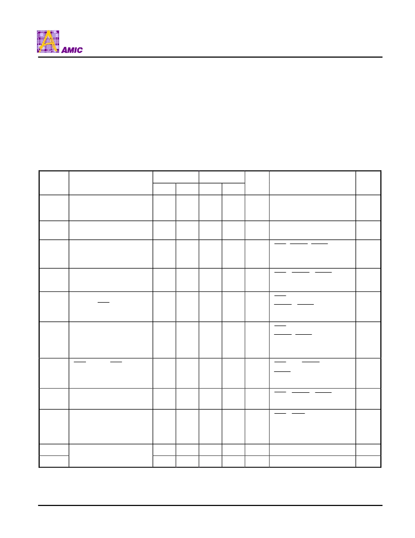
Absolute Maximum Ratings*
Input Voltage (Vin) . . . . . . . . . . . . . . . . . . . . –1.0V to +7.0V
Output Voltage (Vout) . . . . . . . . . . . . . . . . . –1.0V to +7.0V
Power Supply Voltage (VCC) . . . . . . . . . . –1.0V to +7.0V
Operating Temperature (T
OPR
) . . . . . . . . . 0
°
C to +70
°
C
Storage Temperature (T
STG
) . . . . . . . . -55
°
C to +150
°
C
Soldering Temperature X Time (T
SOLDER
) . . . . . . . . . . . . . .
. . . . . . . . . . . . . . . . . . . . . . . . . . . . . . . . . . . . 260
°
C X 10sec
Power Dissipation (P
D
) . . . . . . . . . . . . . . . . . . . . . . . . . 1W
Short Circuit Output Current (Iout) . . . . . . . . . . . . . 50mA
Latch-up Current . . . . . . . . . . . . . . . . . . . . . . . . . . . . 200mA
DC Electrical Characteristics
(VCC = 5.0V
±
10%, VSS = 0V, Ta = 0
°
C to +70
°
C or -40
°
C to +85
°
C)
*Comments
Stresses above those listed under "Absolute Maximum
Ratings" may cause permanent damage to this device.
These are stress ratings only. Functional operation of
this device at these or any other conditions above
those indicated in the operational sections of these
specification is not implied or intended. Exposure to
the absolute maximum rating conditions for extended
periods may affect device reliability.
-45
-50
Symbol
Parameter
Min.
Max.
Min.
Max.
Unit
Test Conditions
Notes
I
IL
Input Leakage Current
-5
+5
-5
+5
μ
A
0V
≤
Vin
≤
VCC
Pins not under
Test = 0V
I
OL
Output Leakage Current
-5
+5
-5
+5
μ
A
D
OUT
disabled,
0V
≤
Vout
≤
VCC
I
CC1
Operating Power Supply
Current
-
120
-
115
mA
RAS,
UCAS
,
LCAS
and
Address cycling;
t
RC
= min.
1, 2
I
CC2
TTL Supply Current Supply
Current
-
1.0
-
1.0
mA
RAS=
UCAS
=
LCAS
= V
IH
I
CC3
Average Power Supply
Current, RAS Refresh
Mode
-
120
-
115
mA
RAS and Address cycling,
UCAS
=
LCAS
= V
IH
,
t
RC
= min.
1
I
CC4
EDO Page Mode Average
Power Supply Current
-
120
-
115
mA
RAS and address = V
IL
,
UCAS
,
LCAS
and
Address cycling;
t
PC
= min.
1, 2
I
CC5
CAS-before-RAS Refresh
Power Supply Current
-
120
-
115
mA
RAS and
UCAS
or
LCAS
cycling;
t
RC
= min.
1
I
CC6
CMOS Standby Power
Supply Current
-
1.0
-
1.0
mA
RAS=
UCAS
=
LCAS
=
VCC - 0.2V
I
CC7
Self Refresh Mode Current
-
1.5
-
1.5
mA
RAS=
CAS
≤
VSS+0.2V
All other input high levels are
VCC-0.2V or input low levels
are VSS +0.2V
V
OH
2.4
-
2.4
-
V
I
OUT
= -5.0mA
V
OL
Output Voltage
-
0.4
-
0.4
V
I
OUT
= 4.2mA
相關PDF資料 |
PDF描述 |
|---|---|
| A420616S-45 | 1M X 16 CMOS DYNAMIC RAM WITH EDO PAGE MODE |
| A420616S-50 | 1M X 16 CMOS DYNAMIC RAM WITH EDO PAGE MODE |
| A420616V-50 | 1M X 16 CMOS DYNAMIC RAM WITH EDO PAGE MODE |
| A420616V-50U | 1M X 16 CMOS DYNAMIC RAM WITH EDO PAGE MODE |
| A420616V-45 | VGA VIDEO CABLE W/ FERRITE CORE,75 FT, MF |
相關代理商/技術參數(shù) |
參數(shù)描述 |
|---|---|
| A420616S-45 | 制造商:AMICC 制造商全稱:AMIC Technology 功能描述:1M X 16 CMOS DYNAMIC RAM WITH EDO PAGE MODE |
| A420616S-50 | 制造商:AMICC 制造商全稱:AMIC Technology 功能描述:1M X 16 CMOS DYNAMIC RAM WITH EDO PAGE MODE |
| A420616V-45 | 制造商:AMICC 制造商全稱:AMIC Technology 功能描述:1M X 16 CMOS DYNAMIC RAM WITH EDO PAGE MODE |
| A420616V-45U | 制造商:AMICC 制造商全稱:AMIC Technology 功能描述:1M X 16 CMOS DYNAMIC RAM WITH EDO PAGE MODE |
| A420616V-50 | 制造商:AMICC 制造商全稱:AMIC Technology 功能描述:1M X 16 CMOS DYNAMIC RAM WITH EDO PAGE MODE |
發(fā)布緊急采購,3分鐘左右您將得到回復。