- 鎮ㄧ従鍦ㄧ殑浣嶇疆锛�璨疯常IC缍� > PDF鐩寗4489 > A3P400-1FGG256I (Microsemi SoC)IC FPGA 1KB FLASH 400K 256-FBGA PDF璩囨枡涓嬭級
鍙冩暩璩囨枡
| 鍨嬭櫉锛� | A3P400-1FGG256I |
| 寤犲晢锛� | Microsemi SoC |
| 鏂囦欢闋佹暩锛� | 149/220闋� |
| 鏂囦欢澶у皬锛� | 0K |
| 鎻忚堪锛� | IC FPGA 1KB FLASH 400K 256-FBGA |
| 妯欐簴鍖呰锛� | 90 |
| 绯诲垪锛� | ProASIC3 |
| RAM 浣嶇附瑷堬細 | 55296 |
| 杓稿叆/杓稿嚭鏁革細 | 178 |
| 闁€鏁革細 | 400000 |
| 闆绘簮闆诲锛� | 1.425 V ~ 1.575 V |
| 瀹夎椤炲瀷锛� | 琛ㄩ潰璨艰 |
| 宸ヤ綔婧害锛� | -40°C ~ 85°C |
| 灏佽/澶栨锛� | 256-LBGA |
| 渚涙噳鍟嗚ō鍌欏皝瑁濓細 | 256-FPBGA锛�17x17锛� |
绗�1闋�绗�2闋�绗�3闋�绗�4闋�绗�5闋�绗�6闋�绗�7闋�绗�8闋�绗�9闋�绗�10闋�绗�11闋�绗�12闋�绗�13闋�绗�14闋�绗�15闋�绗�16闋�绗�17闋�绗�18闋�绗�19闋�绗�20闋�绗�21闋�绗�22闋�绗�23闋�绗�24闋�绗�25闋�绗�26闋�绗�27闋�绗�28闋�绗�29闋�绗�30闋�绗�31闋�绗�32闋�绗�33闋�绗�34闋�绗�35闋�绗�36闋�绗�37闋�绗�38闋�绗�39闋�绗�40闋�绗�41闋�绗�42闋�绗�43闋�绗�44闋�绗�45闋�绗�46闋�绗�47闋�绗�48闋�绗�49闋�绗�50闋�绗�51闋�绗�52闋�绗�53闋�绗�54闋�绗�55闋�绗�56闋�绗�57闋�绗�58闋�绗�59闋�绗�60闋�绗�61闋�绗�62闋�绗�63闋�绗�64闋�绗�65闋�绗�66闋�绗�67闋�绗�68闋�绗�69闋�绗�70闋�绗�71闋�绗�72闋�绗�73闋�绗�74闋�绗�75闋�绗�76闋�绗�77闋�绗�78闋�绗�79闋�绗�80闋�绗�81闋�绗�82闋�绗�83闋�绗�84闋�绗�85闋�绗�86闋�绗�87闋�绗�88闋�绗�89闋�绗�90闋�绗�91闋�绗�92闋�绗�93闋�绗�94闋�绗�95闋�绗�96闋�绗�97闋�绗�98闋�绗�99闋�绗�100闋�绗�101闋�绗�102闋�绗�103闋�绗�104闋�绗�105闋�绗�106闋�绗�107闋�绗�108闋�绗�109闋�绗�110闋�绗�111闋�绗�112闋�绗�113闋�绗�114闋�绗�115闋�绗�116闋�绗�117闋�绗�118闋�绗�119闋�绗�120闋�绗�121闋�绗�122闋�绗�123闋�绗�124闋�绗�125闋�绗�126闋�绗�127闋�绗�128闋�绗�129闋�绗�130闋�绗�131闋�绗�132闋�绗�133闋�绗�134闋�绗�135闋�绗�136闋�绗�137闋�绗�138闋�绗�139闋�绗�140闋�绗�141闋�绗�142闋�绗�143闋�绗�144闋�绗�145闋�绗�146闋�绗�147闋�绗�148闋�鐣跺墠绗�149闋�绗�150闋�绗�151闋�绗�152闋�绗�153闋�绗�154闋�绗�155闋�绗�156闋�绗�157闋�绗�158闋�绗�159闋�绗�160闋�绗�161闋�绗�162闋�绗�163闋�绗�164闋�绗�165闋�绗�166闋�绗�167闋�绗�168闋�绗�169闋�绗�170闋�绗�171闋�绗�172闋�绗�173闋�绗�174闋�绗�175闋�绗�176闋�绗�177闋�绗�178闋�绗�179闋�绗�180闋�绗�181闋�绗�182闋�绗�183闋�绗�184闋�绗�185闋�绗�186闋�绗�187闋�绗�188闋�绗�189闋�绗�190闋�绗�191闋�绗�192闋�绗�193闋�绗�194闋�绗�195闋�绗�196闋�绗�197闋�绗�198闋�绗�199闋�绗�200闋�绗�201闋�绗�202闋�绗�203闋�绗�204闋�绗�205闋�绗�206闋�绗�207闋�绗�208闋�绗�209闋�绗�210闋�绗�211闋�绗�212闋�绗�213闋�绗�214闋�绗�215闋�绗�216闋�绗�217闋�绗�218闋�绗�219闋�绗�220闋�
ProASIC3 DC and Switching Characteristics
2-20
Revision 13
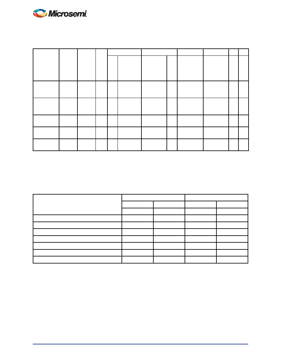
Table 2-20 Summary of Maximum and Minimum DC Input and Output Levels Applicable to Commercial and
Industrial Conditions鈥擲oftware Default Settings
Applicable to Standard I/O Banks
I/O Standard
Drive
Strength
Equiv.
Software
Default
Drive
Strength
Option2
Slew
Rate
VIL
VIH
VOL
VOH
IOL1 IOH1
Min.
V
Max.
V
Min.
V
Max.
V
Max.
V
Min.
VmA mA
3.3 V LVTTL /
3.3 V
LVCMOS
8 mA
High 鈥�0.3
0.8
2
3.6
0.4
2.4
8
3.3 V
LVCMOS
Wide Range3
100 A
8 mA
High 鈥�0.3
0.8
2
3.6
0.2
VCCI 鈥� 0.2
0.1 0.1
2.5 V
LVCMOS
8 mA
High 鈥�0.3
0.7
1.7
3.6
0.7
1.7
8
1.8 V
LVCMOS
4 mA
High 鈥�0.3 0.35 * VCCI 0.65 * VCCI 3.6
0.45
VCCI 鈥� 0.45
4
1.5 V
LVCMOS
2 mA
High 鈥�0.3 0.35 * VCCI 0.65 * VCCI 3.6 0.25 * VCCI 0.75 * VCCI
2
Notes:
1. Currents are measured at 85掳C junction temperature.
2. Please note that 3.3 V LVCMOS wide range is applicable to 100 A drive strength only. The configuration will NOT
operate at the equivalent software default drive strength. These values are for Normal Ranges ONLY.
3. All LVCMOS 3.3 V software macros support LVCMOS 3.3 V wide range as specified in the JESD-8B specification.
Table 2-21 Summary of Maximum and Minimum DC Input Levels
Applicable to Commercial and Industrial Conditions
DC I/O Standards
Commercial1
Industrial2
IIL3
IIH4
IIL3
IIH4
A
3.3 V LVTTL / 3.3 V LVCMOS
10
15
3.3 V LVCMOS Wide Range
10
15
2.5 V LVCMOS
10
15
1.8 V LVCMOS
10
15
1.5 V LVCMOS
10
15
3.3 V PCI
10
15
3.3 V PCI-X
10
15
Notes:
1. Commercial range (0掳C < TA < 70掳C)
2. Industrial range (鈥�40掳C < TA < 85掳C)
3. IIL is the input leakage current per I/O pin over recommended operation conditions where
鈥�0.3V < VIN <VIL.
4. IIH is the input leakage current per I/O pin over recommended operating conditions VIH < VIN < VCCI. Input current is
larger when operating outside recommended ranges.
鐩搁棞PDF璩囨枡 |
PDF鎻忚堪 |
|---|---|
| M1A3P400-1FG256I | IC FPGA 1KB FLASH 400K 256-FBGA |
| A3P400-1FG256I | IC FPGA 1KB FLASH 400K 256-FBGA |
| A54SX08A-FG144A | IC FPGA SX 12K GATES 144-FBGA |
| A54SX08A-FGG144A | IC FPGA SX 12K GATES 144-FBGA |
| IDT71V424S10YG8 | IC SRAM 4MBIT 10NS 36SOJ |
鐩搁棞浠g悊鍟�/鎶€琛撳弮鏁� |
鍙冩暩鎻忚堪 |
|---|---|
| A3P400-1FGG484 | 鍔熻兘鎻忚堪:IC FPGA 1KB FLASH 400K 484-FBGA RoHS:鏄� 椤炲垾:闆嗘垚闆昏矾 (IC) >> 宓屽叆寮� - FPGA锛堢従鍫村彲绶ㄧ▼闁€闄e垪锛� 绯诲垪:ProASIC3 妯欐簴鍖呰:90 绯诲垪:ProASIC3 LAB/CLB鏁�:- 閭忚集鍏冧欢/鍠厓鏁�:- RAM 浣嶇附瑷�:36864 杓稿叆/杓稿嚭鏁�:157 闁€鏁�:250000 闆绘簮闆诲:1.425 V ~ 1.575 V 瀹夎椤炲瀷:琛ㄩ潰璨艰 宸ヤ綔婧害:-40°C ~ 125°C 灏佽/澶栨:256-LBGA 渚涙噳鍟嗚ō鍌欏皝瑁�:256-FPBGA锛�17x17锛� |
| A3P400-1FGG484I | 鍔熻兘鎻忚堪:IC FPGA 1KB FLASH 400K 484-FBGA RoHS:鏄� 椤炲垾:闆嗘垚闆昏矾 (IC) >> 宓屽叆寮� - FPGA锛堢従鍫村彲绶ㄧ▼闁€闄e垪锛� 绯诲垪:ProASIC3 妯欐簴鍖呰:90 绯诲垪:ProASIC3 LAB/CLB鏁�:- 閭忚集鍏冧欢/鍠厓鏁�:- RAM 浣嶇附瑷�:36864 杓稿叆/杓稿嚭鏁�:157 闁€鏁�:250000 闆绘簮闆诲:1.425 V ~ 1.575 V 瀹夎椤炲瀷:琛ㄩ潰璨艰 宸ヤ綔婧害:-40°C ~ 125°C 灏佽/澶栨:256-LBGA 渚涙噳鍟嗚ō鍌欏皝瑁�:256-FPBGA锛�17x17锛� |
| A3P400-1PQ144 | 鍒堕€犲晢:ACTEL 鍒堕€犲晢鍏ㄧū:Actel Corporation 鍔熻兘鎻忚堪:ProASIC3 Flash Family FPGAs |
| A3P400-1PQ144ES | 鍒堕€犲晢:ACTEL 鍒堕€犲晢鍏ㄧū:Actel Corporation 鍔熻兘鎻忚堪:ProASIC3 Flash Family FPGAs |
| A3P400-1PQ144I | 鍒堕€犲晢:ACTEL 鍒堕€犲晢鍏ㄧū:Actel Corporation 鍔熻兘鎻忚堪:ProASIC3 Flash Family FPGAs |
鐧�(f膩)甯冪穵鎬ラ噰璩�锛�3鍒嗛悩宸﹀彸鎮ㄥ皣寰楀埌鍥炲京銆�
