- 您現(xiàn)在的位置:買賣IC網(wǎng) > PDF目錄375100 > A1202LUA-T (Allegro MicroSystems, Inc.) Continuous-Time Bipolar Switch Family PDF資料下載
參數(shù)資料
| 型號: | A1202LUA-T |
| 廠商: | Allegro MicroSystems, Inc. |
| 英文描述: | Continuous-Time Bipolar Switch Family |
| 中文描述: | 連續(xù)時間雙極開關(guān)系列 |
| 文件頁數(shù): | 1/13頁 |
| 文件大?。?/td> | 455K |
| 代理商: | A1202LUA-T |
A1201, A1202, A1203, and A1204
A1201-DS, Rev. 2
Worcester, Massachusetts 01615-0036 (508) 853-5000
www.allegromicro.com
115 Northeast Cutoff, Box 15036
Allegro MicroSystems, Inc.
1
3
2
G
V
V
AB SO LUTE MAX MUM RAT NGS
Supply Voltage, V
CC
..........................................
30 V
Reverse-Supply Voltage, V
RCC
........................
–30 V
Output Off Voltage, V
OUT
..................................
30 V
Reverse-Output Voltage, V
ROUT
.....................
–0.5 V
Output Current, I
OUTSINK
...............................
25 mA
Magnetic Flux Density, B.........................
Unlimited
Operating Temperature
Ambient, T
A
, Range E..................
–40oC to 85oC
Ambient, T
A
, Range L................
–40oC to 150oC
Maximum Junction, T
J(max)
........................
165oC
Storage Temperature, T
S
..................
–65oC to 170oC
Continuous-time operation
– Fast power-on time
– Low noise
Stable operation over full operating temperature range
Reverse battery protection
Solid-state reliability
Factory-programmed at end-of-line for optimum performance
Robust EMC performance
High ESD rating
Regulator stability without a bypass capacitor
The Allegro
A1201, A1202, A1203 and A1204 Hall-effect bipolar switches are
next-generation replacements and extension of the popular Allegro A3134, A3133,
and A3132 bipolar switch product line. Overall, the A120x family, produced with
BiCMOS technology, consists of continuous-time devices that feature fast power-
on time and low-noise operation. Device programming is performed after packag-
ing, to ensure increased switchpoint accuracy by eliminating offsets that can be
induced by package stress. Unique Hall element geometries and low-offset ampli-
fiers help to minimize noise and to reduce the residual offset voltage normally
caused by device overmolding, temperature excursions, and thermal stress.
The A120x Hall-effect bipolar switches include the following on a single silicon
chip: voltage regulator, Hall-voltage generator, small-signal amplifier, Schmitt
trigger, and NMOS output transistor. The integrated voltage regulator permits
operation from 3.8 to 24 V. The extensive on-board protection circuitry makes
possible a ±30 V absolute maximum voltage rating for superior protection in auto-
motive and motor commutation applications, without adding external components.
All devices in the family are identical, except for magnetic switchpoints.
The small geometries of the BiCMOS process allow these devices to be pro-
vided in ultrasmall packages. The package styles available provide magnetically
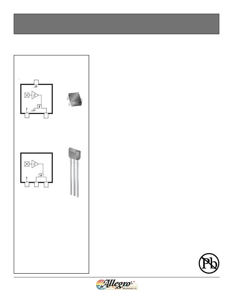
optimized solutions for most applications. Package LH is a SOT23W, a miniature
low-profile surface-mount package, while package UA is a three-lead ultramini
SIP for through-hole mounting. Each package is lead (Pb) free, with 100% matte
tin plated leadframes.
Continuous-Time Bipolar Switch Family
Features and Benefits
Package UA, 3-pin SIP
Package LH, 3-pin Surface Mount
1
2
3
1
2
3
G
V
V
3
12
相關(guān)PDF資料 |
PDF描述 |
|---|---|
| A1201 | Continuous-Time Bipolar Switch Family |
| A1201EUA-T | Continuous-Time Bipolar Switch Family |
| A1202 | Continuous-Time Bipolar Switch Family |
| A1202ELHLT-T | Continuous-Time Bipolar Switch Family |
| A1202EUA-T | Continuous-Time Bipolar Switch Family |
相關(guān)代理商/技術(shù)參數(shù) |
參數(shù)描述 |
|---|---|
| A1202P2 10 | 制造商:Thomas & Betts 功能描述:SS A1202P210 COMBO CHANNEL SIDE HOL |
| A1202W 20 | 制造商:Thomas & Betts 功能描述:A1200 BACK-TO-BACK WELDED |
| A1202W 20PG | 制造商:Thomas & Betts 功能描述:BACK-TO-BACK WELDED PRE-GALV STRUT |
| A1202W 27PG | 制造商:Thomas & Betts 功能描述:COMBINATION CHANNEL |
| A1203 | 制造商:Quick 功能描述:QFP 35 X 35NOZZLE FOR QUICK957/957D |
發(fā)布緊急采購,3分鐘左右您將得到回復(fù)。