- 您現(xiàn)在的位置:買賣IC網(wǎng) > PDF目錄25569 > 9LPRS436CKLF (INTEGRATED DEVICE TECHNOLOGY INC) SPECIALTY MICROPROCESSOR CIRCUIT, PQCC48 PDF資料下載
參數(shù)資料
| 型號: | 9LPRS436CKLF |
| 廠商: | INTEGRATED DEVICE TECHNOLOGY INC |
| 元件分類: | 微控制器/微處理器 |
| 英文描述: | SPECIALTY MICROPROCESSOR CIRCUIT, PQCC48 |
| 封裝: | 6 X 6 MM, 0.40 MM PITCH, ROHS COMPLIANT, PLASTIC, MLF-48 |
| 文件頁數(shù): | 19/20頁 |
| 文件大小: | 195K |
| 代理商: | 9LPRS436CKLF |
IDT
Low Power Clock for Intel Atom-Based Systems
1561C — 08/24/11
9LPRS436C
Low Power Clock for Intel Atom
-Based Systems
8
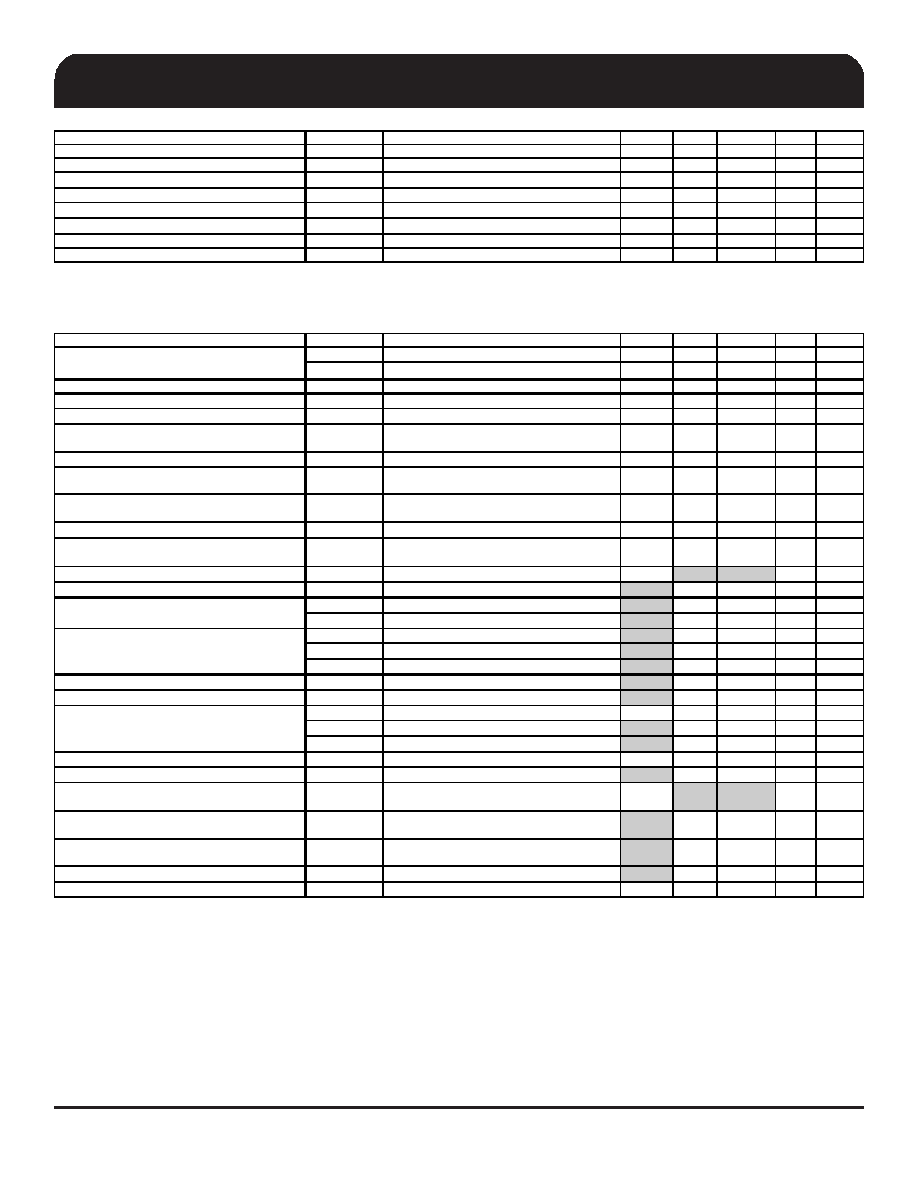
Electrical Characteristics - Absolute Maximum Ratings
PARAMETER
SYMBOL
C OND ITIONS
MIN
TYP
MAX
UNITS NOTES
3.3V Core Supply Voltage
VDDA
4.6
V
1,2
3.3V Logic Supply Voltage
VDD
4.6
V
1,2
Input Low Voltage
VIL
GND-0 .5
V
1
Input High Voltage
VIH
Except for SMBus interface
VDD+0.5V
V
1
Input High Voltage
V
IHSMB
SMBus clock and da ta pins
5.5V
V
1
Storage Temperature
Ts
-65
150
°C1
C ase Temperature
Tcase
115
°C
1
Input ESD protection
ESD prot
Human Body Model
2000
V
1
1Guaranteed by design and characterization, not 100% tested in production.
2 Operation under these conditions is neither implied nor guaranteed.
Electrical Characteristics - Input/Supply/Common Output DC Parameters
PARAMETER
SYMBOL
CONDITIONS
MIN
TYP
MAX
UNITS
Notes
T
amb C
Standard Device
0
85
°C
Tam bI
Industrial Temperature R ange Device
-40
85
°C
Supply VoltageVDDxxx
Supply Voltage
3.135
3.465
V
Input High Voltage
VIHSE
Single-ended 3.3V inputs
2
VDD + 0.3
V
7
Input Low Voltage
VILSE
Single-ended 3.3V inputs
VSS - 0.3
0.8
V
7
FS(4:3) Input High Voltage
V
IH_F S4
Single-ended 3.3V FS(4:3) Inputs
2
VDD + 0.3
V
FS(4:3) Input Low Voltage
V
IL_ FS4
Single-ended 3.3V FS(4:3) Inputs
V
SS - 0.3
0.8
V
Low Threshold Input-
High Voltage
VIH_FS
3.3 V +/-5%
0.7
VDD+0.3
V
Low Threshold Input-
Low Voltage
VIL_FS
3.3 V +/-5%
VSS - 0.3
0.35
V
Input Leakage Current
IIN
VIN = VDD , VIN = GND
-5
5
uA
6
Input Leakage Current
I
INRES
Inputs with pull up or pull down resistors
VIN = VDD , VIN = GND
-200
200
uA
Output High Voltage
VOHSE
Single-ended outputs, IOH = -1mA
2.4
V
5
Output Low Voltage
VOLSE
Single-ended outputs, IOL = 1 mA
0.4
V
5
I
DDVD D3.3
Full Active, C
L = Full load ; IDD 3 .3V
106
115
mA
IDDVDDSUSP3 .3
Full Active, CL = Full load; IDD 3.3V
12
15
mA
I
D DPD VDD3 .3
3.3V Main Rail
0
mA
IDDPDSUSP3.3w
VDD_SUSP Rail. 25MHz Running (WOL)
12
15
mA
I
DD PDSU SP3.3
VDD_SUSP Rail. 25MHz Off
3
4
mA
Input Frequency
F
i
V
DD = 3. 3 V
27
MHz
8
Pin Inductance
Lpin
7nH
C
IN
Logic Inputs
1.5
5
pF
COUT
Output pin capacitance
6
pF
C
IN X
X1 & X2 pins
6
pF
SMBus Voltage
V
DD
2.7
5.5
V
Low-level Output Voltage
VOLSMB
@ IPUL LUP
0.4
V
Current sinking at
VOLSM B = 0.4 V
I
PULLU P
SMB Data Pin
4
mA
SCLK/SDATA
Clock/Data Rise Time
TRI2C
(Max VIL - 0.15) to
(Min VIH + 0.15)
1000
ns
SCLK/SDATA
Clock/D ata Fall Time
TFI2C
(Min VIH + 0.15) to
(Max VIL - 0.15)
300
ns
Maximum SMBus Operating Frequency
FSMBUS
100
kH z
Spread Spectrum Modulation Frequency
f
SSM OD
Triangular Modulation
30
32.5
33
kH z
1 Operation at these points is not recommended
4 Operation under these conditions is nei ther implied, nor guaranteed.
5S ignal is required to be monotonic in this region.
6 Input leakage current does not include inputs with pull-up or pull-down resistors
Ambient Operating Temp
Operating Supply Current
Powerdown Current
Input Capacitance
NOTES on DC Parameters: (unless otherwise noted, guaranteed by design and characterization, not 100% tested in production).
2 Maximum VIH is not to exceed VDD
3 Human Body Model
8 For margining purposes only. Normal operation should have Fin = 25MHz +/-50ppm
7 3.3V referenced inputs are: PCI&P CIEX_STOP #, CPU_STOP#, ITP_EN, SCLK, SDATA, VTT_PWR_GD/PD#, SEL12_48# and PEREQ# inputs if selected.
相關PDF資料 |
PDF描述 |
|---|---|
| 9LPRS436CGLF | SPECIALTY MICROPROCESSOR CIRCUIT, PDSO48 |
| 9LPRS436CKLFT | SPECIALTY MICROPROCESSOR CIRCUIT, PQCC48 |
| 9LPRS436CKILFT | SPECIALTY MICROPROCESSOR CIRCUIT, PQCC48 |
| 9LPRS436CKILF | SPECIALTY MICROPROCESSOR CIRCUIT, PQCC48 |
| 9LPRS436CGLFT | SPECIALTY MICROPROCESSOR CIRCUIT, PDSO48 |
相關代理商/技術參數(shù) |
參數(shù)描述 |
|---|---|
| 9LPRS436CKLFT | 功能描述:時鐘合成器/抖動清除器 ATOM NETTOP/NETBOOK RoHS:否 制造商:Skyworks Solutions, Inc. 輸出端數(shù)量: 輸出電平: 最大輸出頻率: 輸入電平: 最大輸入頻率:6.1 GHz 電源電壓-最大:3.3 V 電源電壓-最小:2.7 V 封裝 / 箱體:TSSOP-28 封裝:Reel |
| 9LPRS437AFLF | 制造商:Integrated Device Technology Inc 功能描述:IDT 9LPRS437AFLF GENERAL PURPOSE SEMICONDUCTORS - Rail/Tube 制造商:Integrated Device Technology Inc 功能描述:IDT 9LPRS437AFLF General Purpose Semiconductors |
| 9LPRS437AFLFT | 制造商:Integrated Device Technology Inc 功能描述:IDT 9LPRS437AFLFT SEMICONDUCTORS - Tape and Reel 制造商:Integrated Device Technology Inc 功能描述:IDT 9LPRS437AFLFT Semiconductors |
| 9LPRS462AGLF | 功能描述:時鐘合成器/抖動清除器 RoHS:否 制造商:Skyworks Solutions, Inc. 輸出端數(shù)量: 輸出電平: 最大輸出頻率: 輸入電平: 最大輸入頻率:6.1 GHz 電源電壓-最大:3.3 V 電源電壓-最小:2.7 V 封裝 / 箱體:TSSOP-28 封裝:Reel |
| 9LPRS462AGLFT | 功能描述:時鐘合成器/抖動清除器 RoHS:否 制造商:Skyworks Solutions, Inc. 輸出端數(shù)量: 輸出電平: 最大輸出頻率: 輸入電平: 最大輸入頻率:6.1 GHz 電源電壓-最大:3.3 V 電源電壓-最小:2.7 V 封裝 / 箱體:TSSOP-28 封裝:Reel |
發(fā)布緊急采購,3分鐘左右您將得到回復。