- 您現(xiàn)在的位置:買賣IC網(wǎng) > PDF目錄25565 > 9ERS3165BGILFT (INTEGRATED DEVICE TECHNOLOGY INC) 200 MHz, PROC SPECIFIC CLOCK GENERATOR, PDSO64 PDF資料下載
參數(shù)資料
| 型號: | 9ERS3165BGILFT |
| 廠商: | INTEGRATED DEVICE TECHNOLOGY INC |
| 元件分類: | 時鐘產(chǎn)生/分配 |
| 英文描述: | 200 MHz, PROC SPECIFIC CLOCK GENERATOR, PDSO64 |
| 封裝: | 6.10 MM, 0.50 MM PITCH, ROHS COMPLIANT, TSSOP-64 |
| 文件頁數(shù): | 11/26頁 |
| 文件大?。?/td> | 319K |
| 代理商: | 9ERS3165BGILFT |
IDTTM
Embedded 64-Pin Industrial Temperature Range CK505 Compatible Clock
1613B—01/25/10
ICS9ERS3165
Embedded 64-Pin Industrial Temperature Range CK505 Compatible Clock
19
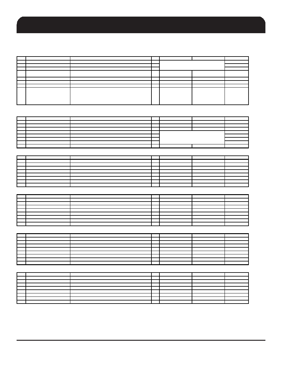
Byte 0 FS Readback & PLL Selection Register
Bit
Name
Description
Type
0
1
Default
7FSLC
CPU Freq. Sel. Bit (Most Significant)
RLatch
6FSLB
CPU Freq. Sel. Bit
RLatch
5FSLA
CPU Freq. Sel. Bit (Least Significant)
RLatch
4
iAMT_EN
Set via SMBus or dynamically by CK505 if detects dynamic M1
R
Legacy Mode
iAMT Enabled
iAMT power on
status
3Reserved
Reserved
RW
0
2
SRC_Main_SEL
Select source for SRC Main
RW
SRC Main = PLL5
SRC Main = PLL2
0
1
SATA_SEL
Select source for SATA clock
RW
SATA = SRC_Main
SATA = PLL3
0
PD_Restore
1 = on Power Down de-assert return to last known state
0 = clear all SMBus configurations as if cold power-on and go to
latches open state
This bit is ignored and treated at '1' if device is in iAMT mode.
RW
Configuration Not Saved
Configuration Saved
1
Byte 1 PLL1 Quick Config Register
Note 1 : When 27_Select pin = 0, B1b7 PWD = 1; When 27_Select pin = 1, PWD = 0
Bit
Name
Description
Type
0
1
Default
7
SRC0_SEL
Select SRC0 or DOT96
RW
SRC0
DOT96
Note 1
6
PLL5_SSC_SEL
Select 0.5% down or center SSC
RW
Down spread
Center spread
0
5
PLL2_SSC SEL
Select 0.5% center or down SSC
RW
Down
Center
0
4
PLL1_CF3
PLL1 Quick Config Bit 3
RW
0
3
PLL1_CF2
PLL1 Quick Config Bit 2
RW
0
2
PLL1_CF1
PLL1 Quick Config Bit 1
RW
1
PLL1_CF0
PLL1 Quick Config Bit 0
RW
0
PCI_SEL
RW
PCI from PLL5
PCI from SRC_MAIN
1
Byte 2 Single Ended Output Enable Register
Bit
Name
Description
Type
0
1
Default
7REF_OE
Output enable for REF
RW
Output Disabled
Output Enabled
1
6
USB_OE
Output enable for USB
RW
Output Disabled
Output Enabled
1
5
PCIF5_OE
Output enable for PCI5
RW
Output Disabled
Output Enabled
1
4PCI4_OE
Output enable for PCI4
RW
Output Disabled
Output Enabled
1
3PCI3_OE
Output enable for PCI3
RW
Output Disabled
Output Enabled
1
2PCI2_OE
Output enable for PCI2
RW
Output Disabled
Output Enabled
1
1PCI1_OE
Output enable for PCI1
RW
Output Disabled
Output Enabled
1
0
PCI0_OE
Output enable for PCI0
RW
Output Disabled
Output Enabled
1
Byte 3 SRC Output Enable Register
Bit
Name
Description
Type
0
1
Default
7
SRC11_OE
Output enable for SRC11
RW
Output Disabled
Output Enabled
1
6
SRC10_OE
Output enable for SRC10
RW
Output Disabled
Output Enabled
1
5
SRC9_OE
Output enable for SRC9
RW
Output Disabled
Output Enabled
1
4
SRC8/ITP_OE
Output enable for SRC8 or ITP
RW
Output Disabled
Output Enabled
1
3
SRC7_OE
Output enable for SRC7
RW
Output Disabled
Output Enabled
1
2
SRC6_OE
Output enable for SRC6
RW
Output Disabled
Output Enabled
1
Reserved
RW
-
1
0
SRC4_OE
Output enable for SRC4
RW
Output Disabled
Output Enabled
1
Byte 4 SRC/CPU/DOT Output Enable & Spread Spectrum Disable Register
Bit
Name
Description
Type
0
1
Default
7
SRC3_OE
Output enable for SRC3
RW
Output Disabled
Output Enabled
1
6
SATA/SRC2_OE
Output enable for SATA/SRC2
RW
Output Disabled
Output Enabled
1
5
SRC1_OE
Output enable for SRC1
RW
Output Disabled
Output Enabled
1
4
SRC0/DOT96_OE
Output enable for SRC0/DOT96
RW
Output Disabled
Output Enabled
1
3
CPU1_OE
Output enable for CPU1
RW
Output Disabled
Output Enabled
1
2CPU0_OE
Output enable for CPU0
RW
Output Disabled
Output Enabled
1
PLL5_SSC_ON
Enable PLL5's spread modulation
RW
Spread Disabled
Spread Enabled
1
0
PLL2_SSC_ON
Enable PLL2's spread modulation
RW
Spread Disabled
Spread Enabled
1
Byte 5 Clock Request Enable/Configuration Register
Bit
Name
Description
Type
0
1
Default
7
CR#_A_EN
Enable CR#_A (clk req) for SRC0 or SRC2
RW
Disable CR#_A
Enable CR#_A
0
6
CR#_A_SEL
Sets CR#_A to control either SRC0 or SRC2
RW
CR#_A -> SRC0
CR#_A -> SRC2
0
5
CR#_B_EN
Enable CR#_B (clk req) for SRC1 or SRC4
RW
Disable CR#_B
Enable CR#_B
0
4
CR#_B_SEL
Sets CR#_B to control either SRC1 or SRC4
RW
CR#_B -> SRC1
CR#_B -> SRC4
0
3CR#_C_EN
Enable CR#_C (clk req) for SRC0 or SRC2
RW
Disable CR#_C
Enable CR#_C
0
2
CR#_C_SEL
Sets CR#_C to control either SRC0 or SRC2
RW
CR#_C -> SRC0
CR#_C -> SRC2
0
1
CR#_D_EN
Enable CR#_D (clk req) for SRC1 or SRC4
RW
Disable CR#_D
Enable CR#_D
0
CR#_D_SEL
Sets CR#_D to control either SRC1 or SRC4
RW
CR#_D -> SRC1
CR#_D -> SRC4
0
See Table 1 : CPU Frequency Select Table
See Table 2: pin 27FIX/LCDT/SRCT_LR1/SE1,
27SS/LCDC/SRCC_LR1/SE2 Configuration
Only applies if Byte 0, bit 2 = 0.
相關PDF資料 |
PDF描述 |
|---|---|
| 9EX21501AKLFT | 21501 SERIES, PLL BASED CLOCK DRIVER, 15 TRUE OUTPUT(S), 0 INVERTED OUTPUT(S), PQCC64 |
| 9EX21501AKLF | 21501 SERIES, PLL BASED CLOCK DRIVER, 15 TRUE OUTPUT(S), 0 INVERTED OUTPUT(S), PQCC64 |
| 9EX21501AKILF | 21501 SERIES, PLL BASED CLOCK DRIVER, 15 TRUE OUTPUT(S), 0 INVERTED OUTPUT(S), PQCC64 |
| 9EX21801AKLF | PLL BASED CLOCK DRIVER, PQCC72 |
| 9EX21801AKLFT | PLL BASED CLOCK DRIVER, PQCC72 |
相關代理商/技術參數(shù) |
參數(shù)描述 |
|---|---|
| 9ERS3165BGLF | 功能描述:時鐘合成器/抖動清除器 EMBEDDED CK505 COMPATIBLE CLOCK RoHS:否 制造商:Skyworks Solutions, Inc. 輸出端數(shù)量: 輸出電平: 最大輸出頻率: 輸入電平: 最大輸入頻率:6.1 GHz 電源電壓-最大:3.3 V 電源電壓-最小:2.7 V 封裝 / 箱體:TSSOP-28 封裝:Reel |
| 9ERS3165BGLFT | 功能描述:時鐘合成器/抖動清除器 EMBEDDED CK505 COMPATIBLE CLOCK RoHS:否 制造商:Skyworks Solutions, Inc. 輸出端數(shù)量: 輸出電平: 最大輸出頻率: 輸入電平: 最大輸入頻率:6.1 GHz 電源電壓-最大:3.3 V 電源電壓-最小:2.7 V 封裝 / 箱體:TSSOP-28 封裝:Reel |
| 9ERS3165BKILF | 功能描述:時鐘合成器/抖動清除器 EMBEDDED CK505 COMPATIBLE CLOCK RoHS:否 制造商:Skyworks Solutions, Inc. 輸出端數(shù)量: 輸出電平: 最大輸出頻率: 輸入電平: 最大輸入頻率:6.1 GHz 電源電壓-最大:3.3 V 電源電壓-最小:2.7 V 封裝 / 箱體:TSSOP-28 封裝:Reel |
| 9ERS3165BKILFT | 功能描述:時鐘合成器/抖動清除器 EMBEDDED CK505 COMPATIBLE CLOCK RoHS:否 制造商:Skyworks Solutions, Inc. 輸出端數(shù)量: 輸出電平: 最大輸出頻率: 輸入電平: 最大輸入頻率:6.1 GHz 電源電壓-最大:3.3 V 電源電壓-最小:2.7 V 封裝 / 箱體:TSSOP-28 封裝:Reel |
| 9ERS3165BKLF | 功能描述:時鐘合成器/抖動清除器 EMBEDDED CK505 COMPATIBLE CLOCK RoHS:否 制造商:Skyworks Solutions, Inc. 輸出端數(shù)量: 輸出電平: 最大輸出頻率: 輸入電平: 最大輸入頻率:6.1 GHz 電源電壓-最大:3.3 V 電源電壓-最小:2.7 V 封裝 / 箱體:TSSOP-28 封裝:Reel |
發(fā)布緊急采購,3分鐘左右您將得到回復。