- 您現在的位置:買賣IC網 > PDF目錄24812 > 935263971112 (NXP SEMICONDUCTORS) SPECIALTY TELECOM CIRCUIT, PDSO28 PDF資料下載
參數資料
| 型號: | 935263971112 |
| 廠商: | NXP SEMICONDUCTORS |
| 元件分類: | 通信及網絡 |
| 英文描述: | SPECIALTY TELECOM CIRCUIT, PDSO28 |
| 封裝: | PLASTIC, SOT-136, SO-28 |
| 文件頁數: | 15/38頁 |
| 文件大小: | 287K |
| 代理商: | 935263971112 |
第1頁第2頁第3頁第4頁第5頁第6頁第7頁第8頁第9頁第10頁第11頁第12頁第13頁第14頁當前第15頁第16頁第17頁第18頁第19頁第20頁第21頁第22頁第23頁第24頁第25頁第26頁第27頁第28頁第29頁第30頁第31頁第32頁第33頁第34頁第35頁第36頁第37頁第38頁
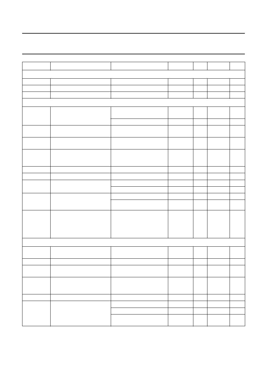
1999 Feb 17
22
Philips Semiconductors
Product specication
Cordless telephone, answering machine
line interface
UBA1707
Electronic hook-switch control (pin EHI)
VIH
HIGH-level input voltage
2.3
VCC + 0.4 V
VIL
LOW-level input voltage
VCC = 3.0 to 5.5 V
GND
0.4
0.3VCC
V
Ibias
input bias current
input level = HIGH
1
2
5
A
Transmit amplier (pins TXI+, TXI
and LN)
Z
i
input impedance
between pins TXI+ and GND
or TXI
and GND
21
k
between pins TXI+ and TXI
36
k
Gv(TX)
voltage gain from TXI+/TXI
to LN
VTXI = 50 mV (RMS)
10.6
11.6
12.6
dB
G
v(TX)(f)
voltage gain variation with
frequency referenced to 1 kHz
f = 300 to 3400 Hz
±0.3
dB
G
v(TX)(T)
voltage gain variation with
temperature referenced to
25
°C
Tamb = 25 to +75 °C
±0.3
dB
CMRR
common mode rejection ratio
65
dB
PSRR
power supply rejection ratio
36
dB
VLN(max)(rms)
maximum sending signal
(RMS value)
Iline = 15 mA; THD = 2%
1.2
1.4
V
Iline = 4 mA; THD = 10%
0.26
V
ViTX(max)(rms)
maximum transmit input
voltage (RMS value) for
2% THD on pin LN
Iline =15mA
0.35
V
Iline =90mA
0.75
V
Vno(LN)
noise output voltage at pin LN
pins TXI+ and TXI
short-circuited through
200
in series with 10 F;
psophometrically weighted
(P53 curve)
74
dBmp
Receive amplier (pins RXI and RXO; bit RXM)
Zi
input impedance between pins
RXI and GND
21
k
Gv(RX)
voltage gain from RXI to RXO
VRXI = 2 mV (RMS)
36.9
37.9
38.9
dB
G
v(RX)(f)
voltage gain variation with
frequency referenced to 1 kHz
f = 300 to 3400 Hz
±0.2
dB
G
v(RX)(T)
voltage gain variation with
temperature referenced to
25
°C
Tamb = 25 to +75 °C
±0.3
dB
PSRR
power supply rejection ratio
68
dB
THD
total harmonic distortion
VRXI = 2 mV (RMS)
0.03
%
VRXI = 12.5 mV (RMS)
2
%
VRXI = 19.5 mV (RMS);
Iline =90mA
2
%
SYMBOL
PARAMETER
CONDITIONS
MIN.
TYP.
MAX.
UNIT
相關PDF資料 |
PDF描述 |
|---|---|
| 935263971118 | SPECIALTY TELECOM CIRCUIT, PDSO28 |
| 08-040831 | OUTLINE AUTO - TANGING MEGAPAC |
| 08-040831-C | OUTLINE AUTO - TANGING MEGAPAC |
| 08-040921 | OUTLINE MINI MEGAPAC STANDARD CHASSIS |
| 08-040921-D | OUTLINE MINI MEGAPAC STANDARD CHASSIS |
相關代理商/技術參數 |
參數描述 |
|---|---|
| 935264217557 | 制造商:NXP Semiconductors 功能描述:SUB ONLY IC |
| 935267356112 | 制造商:NXP Semiconductors 功能描述:IC TEA1507PN |
| 935268081112 | 制造商:NXP Semiconductors 功能描述:SUB ONLY IC |
| 935268721125 | 制造商:NXP Semiconductors 功能描述:Buffer/Line Driver 1-CH Non-Inverting 3-ST CMOS 5-Pin TSSOP T/R |
| 935269304128 | 制造商:ST-Ericsson 功能描述:IC AUDIO CODEC W/TCH SCRN 48LQFP |
發(fā)布緊急采購,3分鐘左右您將得到回復。