- 您現(xiàn)在的位置:買賣IC網(wǎng) > PDF目錄24654 > 933670820652 (NXP SEMICONDUCTORS) HCT SERIES, 8-BIT BIDIRECTIONAL PARALLEL IN PARALLEL OUT SHIFT REGISTER, TRUE OUTPUT, PDIP20 PDF資料下載
參數(shù)資料
| 型號(hào): | 933670820652 |
| 廠商: | NXP SEMICONDUCTORS |
| 元件分類: | 計(jì)數(shù)移位寄存器 |
| 英文描述: | HCT SERIES, 8-BIT BIDIRECTIONAL PARALLEL IN PARALLEL OUT SHIFT REGISTER, TRUE OUTPUT, PDIP20 |
| 封裝: | SOT-146-1, DIP-20 |
| 文件頁(yè)數(shù): | 4/11頁(yè) |
| 文件大小: | 79K |
| 代理商: | 933670820652 |
December 1990
2
Philips Semiconductors
Product specication
8-bit universal shift register; 3-state
74HC/HCT299
FEATURES
Multiplexed inputs/outputs provide improved bit density
Four operating modes:
– shift left
– shift right
– hold (store)
– load data
Operates with output enable or at high-impedance
OFF-state (Z)
3-state outputs drive bus lines directly
Can be cascaded for n-bits word length
Output capability: bus driver (parallel I/Os),
standard (serial outputs)
ICC category: MSI
GENERAL DESCRIPTION
The 74HC/HCT299 are high-speed Si-gate CMOS devices
and are pin compatible with low power Schottky TTL
(LSTTL). They are specified in compliance with JEDEC
standard no. 7A.
The 74HC/HCT299 contain eight edge-triggered D-type
flip-flops and the interstage logic necessary to perform
synchronous shift-right, shift-left, parallel load and hold
operations. The type of operation is determined by the
mode select inputs (S0 and S1), as shown in the mode
select table.
All flip-flop outputs have 3-state buffers to separate these
outputs (I/O0 to I/O7) such, that they can serve as data
inputs in the parallel load mode. The serial outputs (Q0 and
Q7) are used for expansion in serial shifting of longer
words.
A LOW signal on the asynchronous master reset input
(MR) overrides the Sn and clock (CP) inputs and resets the
flip-flops. All other state changes are initiated by the rising
edge of the clock pulse. Inputs can change when the clock
is either state, provided that the recommended set-up and
hold times, relative to the rising edge of CP, are observed.
A HIGH signal on the 3-state output enable inputs (OE1 or
OE2) disables the 3-state buffers and the I/On outputs are
set to the high-impedance OFF-state. In this condition, the
shift, hold, load and reset operations can still occur. The
3-state buffers are also disabled by HIGH signals on both
S0 and S1, when in preparation for a parallel load
operation.
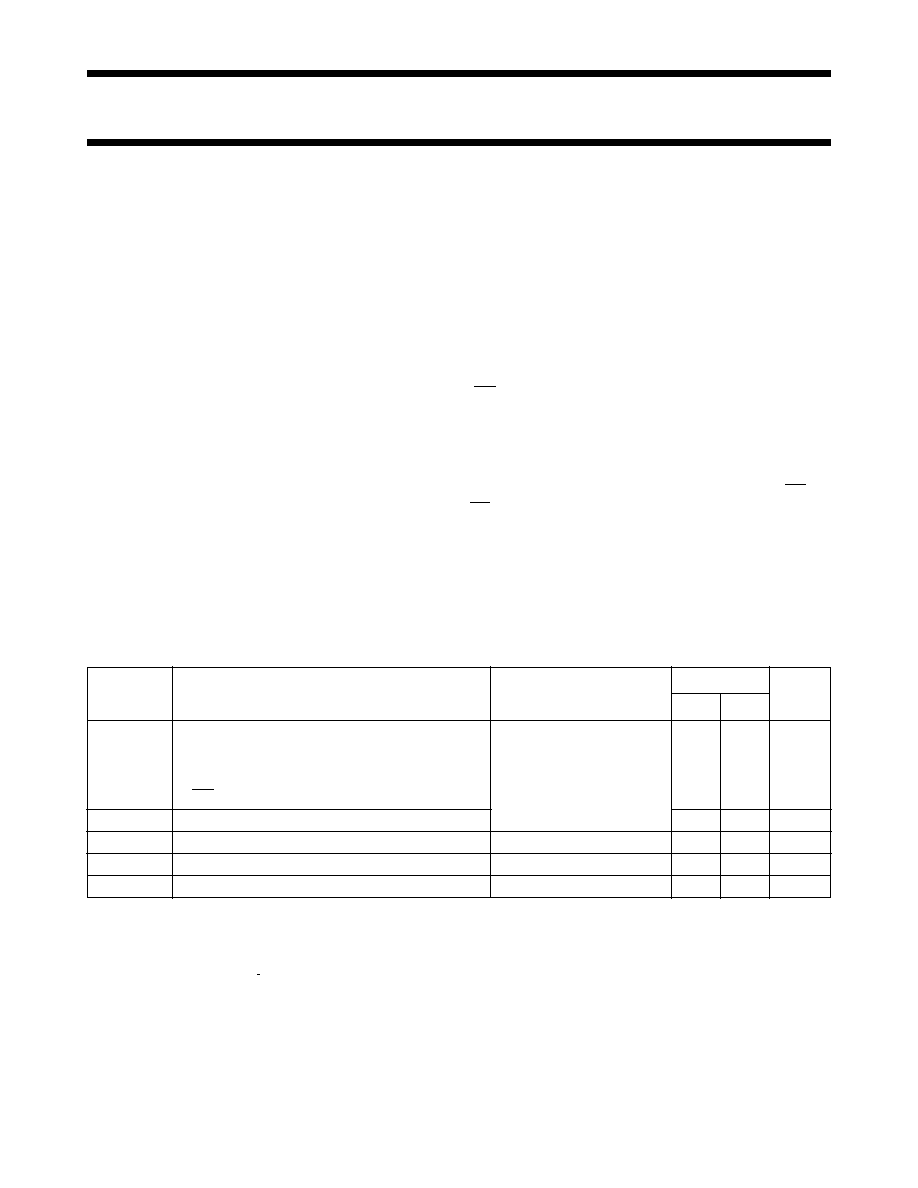
QUICK REFERENCE DATA
GND = 0 V; Tamb =25 °C; tr =tf = 6 ns
SYMBOL
PARAMETER
CONDITIONS
TYPICAL
UNIT
HC
HCT
tPHL/ tPLH
propagation delay
CL = 15 pF; VCC =5 V
CP to Q0, Q7
20
19
ns
CP to I/On
20
19
ns
tPHL
MR to Q0, Q7 or I/On
20
23
ns
fmax
maximum clock frequency
50
46
MHz
CI
input capacitance
3.5
pF
CI/O
input/output capacitance
10
pF
CPD
power dissipation capacitance per package
notes 1 and 2
120
125
pF
Notes
1. CPD is used to determine the dynamic power
dissipation (PD in W):
PD =CPD × VCC2 × fi + ∑ (CL × VCC2 × fo) where:
fi = input frequency in MHz
fo = output frequency in MHz
∑ (CL × VCC2 × fo) = sum of outputs
CL = output load capacitance in pF
VCC = supply voltage in V
2. For HC the condition is VI = GND to VCC
For HCT the condition is VI = GND to VCC 1.5 V
ORDERING INFORMATION
See
“74HC/HCT/HCU/HCMOS Logic Package
Information”.
相關(guān)PDF資料 |
PDF描述 |
|---|---|
| 935189880118 | HCT SERIES, 8-BIT BIDIRECTIONAL PARALLEL IN PARALLEL OUT SHIFT REGISTER, TRUE OUTPUT, PDSO20 |
| 933713540652 | HC/UH SERIES, 8-BIT BIDIRECTIONAL PARALLEL IN PARALLEL OUT SHIFT REGISTER, TRUE OUTPUT, PDSO20 |
| 933670570652 | HC/UH SERIES, 8-BIT BIDIRECTIONAL PARALLEL IN PARALLEL OUT SHIFT REGISTER, TRUE OUTPUT, PDIP20 |
| 933713550653 | HCT SERIES, 8-BIT BIDIRECTIONAL PARALLEL IN PARALLEL OUT SHIFT REGISTER, TRUE OUTPUT, PDSO20 |
| 935189890118 | HC/UH SERIES, 8-BIT BIDIRECTIONAL PARALLEL IN PARALLEL OUT SHIFT REGISTER, TRUE OUTPUT, PDSO20 |
相關(guān)代理商/技術(shù)參數(shù) |
參數(shù)描述 |
|---|---|
| 9336CMG | 制造商:Apex Tool Group 功能描述:6 IN. DIAGONAL CUTTING S J PLIERS W/CO-MOLDED GRIPS, LASER HARDENED EDGES, CDD |
| 9336CVN | 制造商:Apex Tool Group 功能描述:6 IN. DIAGONAL CUTTING SOLID JOINT PLIERS, CUSHION GRIP, CARDED |
| 9336N | 制造商:Apex Tool Group 功能描述:6 IN. DIAGONAL CUTTING, GENERAL PURPOSE SOLID JOINT PLIERS |
| 9336-RED | 制造商: 功能描述: 制造商:undefined 功能描述: |
| 9336SCN | 制造商:Apex Tool Group 功能描述:6 IN. DIAGONAL CUTTING SOLID JOINT PLIERS, CUSHION GRIP |
發(fā)布緊急采購(gòu),3分鐘左右您將得到回復(fù)。