- 您現(xiàn)在的位置:買賣IC網 > PDF目錄375082 > 74LVTH32374 (Fairchild Semiconductor Corporation) Low Voltage 32-Bit D-Type Flip-Flop with 3-STATE Outputs PDF資料下載
參數資料
| 型號: | 74LVTH32374 |
| 廠商: | Fairchild Semiconductor Corporation |
| 英文描述: | Low Voltage 32-Bit D-Type Flip-Flop with 3-STATE Outputs |
| 中文描述: | 低電壓32位D類觸發(fā)器觸發(fā)器3態(tài)輸出 |
| 文件頁數: | 2/6頁 |
| 文件大小: | 77K |
| 代理商: | 74LVTH32374 |
www.fairchildsemi.com
2
7
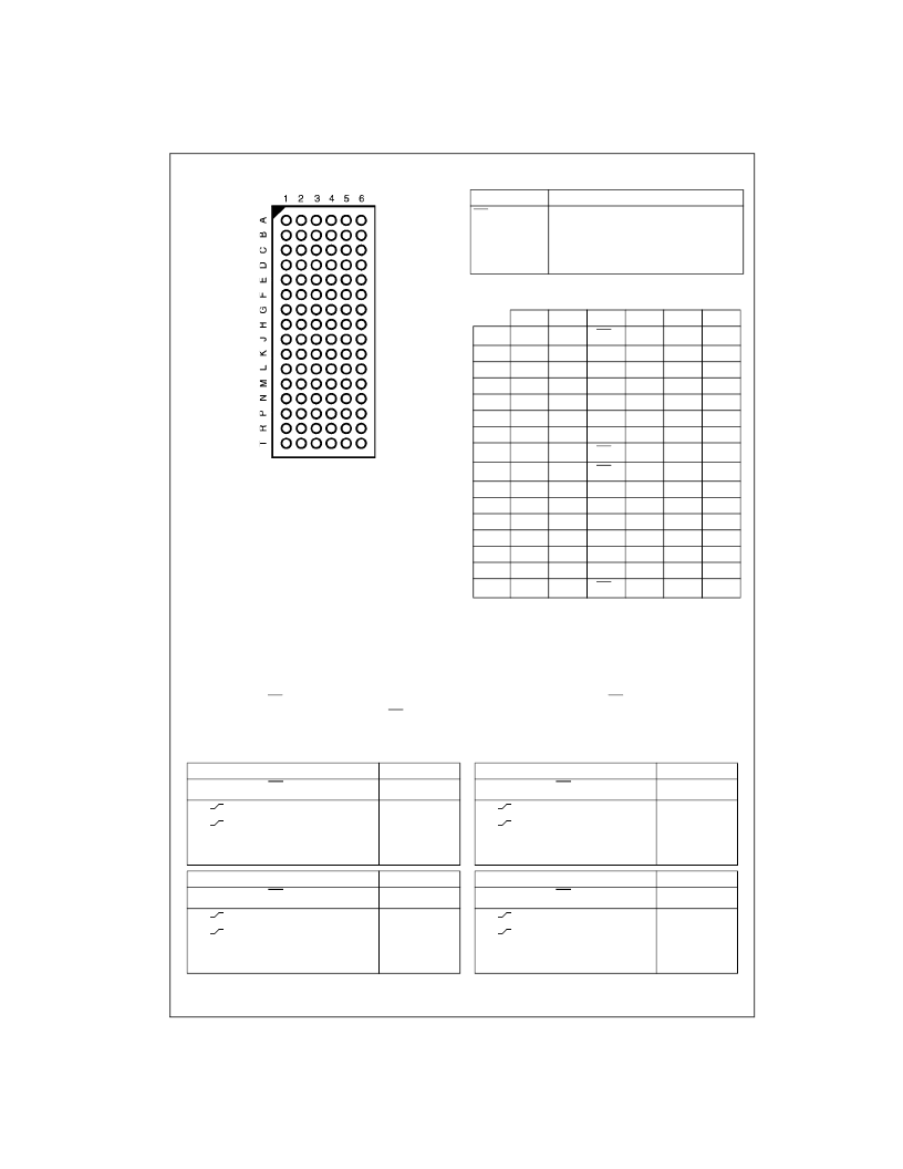
Connection Diagram
(Top Thru View)
Pin Descriptions
FBGA Pin Assignments
Functional Description
The LVT32374 and LVTH32374 consist of thirty-two edge-triggered flip-flops with individual D-type inputs and 3-STATE true
outputs. The device is byte controlled with each byte functioning identically, but independent of the other. The control pins
can be shorted together to obtain full 32-bit operation. Each byte has a buffered clock and buffered Output Enable common
to all flip-flops within that byte. The description which follows applies to each byte. Each flip-flop will store the state of their
individual D-type inputs that meet the setup and hold time requirements on the LOW-to-HIGH Clock (CP
n
) transition. With
the Output Enable (OE
n
) LOW, the contents of the flip-flops are available at the outputs. When OE
n
is HIGH, the outputs go
to the high impedance state. Operation of the OE
n
input does not affect the state of the flip-flops.
Truth Tables
H
=
HIGH Voltage Level
L
=
LOW Voltage Level
X
=
Immaterial
Z
=
HIGH Impedance
O
o
=
Previous O
o
before HIGH-to-LOW of CP
Pin Names
Description
OE
n
CP
n
I
0
–
I
31
O
0
–
O
31
Output Enable Input (Active LOW)
Clock Pulse Input
Inputs
3-STATE Outputs
1
2
3
4
5
6
A
B
C
D
E
F
G
O
1
O
3
O
5
O
7
O
9
O
11
O
13
O
14
O
17
O
19
O
21
O
23
O
25
O
27
O
29
O
30
O
0
O
2
O
4
O
6
O
8
O
10
O
12
O
15
O
16
O
18
O
20
O
22
O
24
O
26
O
28
O
31
OE
1
GND
V
CC1
GND
GND
V
CC1
GND
CP
1
GND
V
CC1
GND
GND
V
CC1
GND
I
0
I
2
I
4
I
6
I
8
I
10
I
12
I
15
I
16
I
18
I
20
I
22
I
24
I
26
I
28
I
31
I
1
I
3
I
5
I
7
I
9
I
11
I
13
I
14
I
17
I
19
I
21
I
23
I
25
I
27
I
29
I
30
H
OE
2
OE
3
GND
V
CC2
GND
GND
V
CC2
GND
CP
2
CP
3
GND
V
CC2
GND
GND
V
CC2
GND
J
K
L
M
N
P
R
T
OE
4
CP
4
Inputs
Outputs
Inputs
Outputs
CP
1
OE
1
L
L
L
H
I
0
–
I
7
H
L
X
X
O
0
–
O
7
H
L
O
o
Z
CP
2
OE
2
L
L
L
H
I
8
–
I
15
H
L
X
X
O
8
–
O
15
H
L
O
o
Z
L
X
L
X
Inputs
Outputs
Inputs
Outputs
CP
3
OE
3
L
L
L
H
I
16
–
I
23
H
L
X
X
O
16
–
O
23
H
L
O
o
Z
CP
4
OE
4
L
L
L
H
I
24
–
I
31
H
L
X
X
O
24
–
O
31
H
L
O
o
Z
L
X
L
X
相關PDF資料 |
PDF描述 |
|---|---|
| 74LVTH32374G | Quadruple Positive-NOR Gates With Schmitt-Trigger Inputs 14-SO -40 to 85 |
| 74LVTH125M | Low Voltage Quad Buffer with 3-STATE Outputs |
| 74LVTH125MTCX_NL | Low Voltage Quad Buffer with 3-STATE Outputs |
| 74LVTH125 | Low Voltage Quad Buffer with 3-STATE Outputs |
| 74LVTH125MTC | 8-Bit Shift Registers With 3-State Output Registers 16-SOIC -40 to 85 |
相關代理商/技術參數 |
參數描述 |
|---|---|
| 74LVTH32374GX | 功能描述:觸發(fā)器 D-Type Flip-Flop LV 32Bit RoHS:否 制造商:Texas Instruments 電路數量:2 邏輯系列:SN74 邏輯類型:D-Type Flip-Flop 極性:Inverting, Non-Inverting 輸入類型:CMOS 輸出類型: 傳播延遲時間:4.4 ns 高電平輸出電流:- 16 mA 低電平輸出電流:16 mA 電源電壓-最大:5.5 V 最大工作溫度:+ 85 C 安裝風格:SMD/SMT 封裝 / 箱體:X2SON-8 封裝:Reel |
| 74LVTH373MTC | 功能描述:閉鎖 Octal Trans Latch RoHS:否 制造商:Micrel 電路數量:1 邏輯類型:CMOS 邏輯系列:TTL 極性:Non-Inverting 輸出線路數量:9 高電平輸出電流: 低電平輸出電流: 傳播延遲時間: 電源電壓-最大:12 V 電源電壓-最小:5 V 最大工作溫度:+ 85 C 最小工作溫度:- 40 C 封裝 / 箱體:SOIC-16 封裝:Reel |
| 74LVTH373MTCX | 功能描述:閉鎖 Octal Trans Latch RoHS:否 制造商:Micrel 電路數量:1 邏輯類型:CMOS 邏輯系列:TTL 極性:Non-Inverting 輸出線路數量:9 高電平輸出電流: 低電平輸出電流: 傳播延遲時間: 電源電壓-最大:12 V 電源電壓-最小:5 V 最大工作溫度:+ 85 C 最小工作溫度:- 40 C 封裝 / 箱體:SOIC-16 封裝:Reel |
| 74LVTH373MTCX_NL | 功能描述:閉鎖 LV OCTAL TRANSP LATCH BH RoHS:否 制造商:Micrel 電路數量:1 邏輯類型:CMOS 邏輯系列:TTL 極性:Non-Inverting 輸出線路數量:9 高電平輸出電流: 低電平輸出電流: 傳播延遲時間: 電源電壓-最大:12 V 電源電壓-最小:5 V 最大工作溫度:+ 85 C 最小工作溫度:- 40 C 封裝 / 箱體:SOIC-16 封裝:Reel |
| 74LVTH373SJ | 功能描述:閉鎖 Octal Trans Latch RoHS:否 制造商:Micrel 電路數量:1 邏輯類型:CMOS 邏輯系列:TTL 極性:Non-Inverting 輸出線路數量:9 高電平輸出電流: 低電平輸出電流: 傳播延遲時間: 電源電壓-最大:12 V 電源電壓-最小:5 V 最大工作溫度:+ 85 C 最小工作溫度:- 40 C 封裝 / 箱體:SOIC-16 封裝:Reel |
發(fā)布緊急采購,3分鐘左右您將得到回復。