- 您現(xiàn)在的位置:買賣IC網(wǎng) > PDF目錄222840 > 74LVTH182512DGGRG4 (TEXAS INSTRUMENTS INC) LVT SERIES, DUAL 9-BIT BOUNDARY SCAN REG TRANSCEIVER, TRUE OUTPUT, PDSO64 PDF資料下載
參數(shù)資料
| 型號(hào): | 74LVTH182512DGGRG4 |
| 廠商: | TEXAS INSTRUMENTS INC |
| 元件分類: | 總線收發(fā)器 |
| 英文描述: | LVT SERIES, DUAL 9-BIT BOUNDARY SCAN REG TRANSCEIVER, TRUE OUTPUT, PDSO64 |
| 封裝: | GREEN, PLASTIC, TSSOP-64 |
| 文件頁數(shù): | 16/38頁 |
| 文件大小: | 735K |
| 代理商: | 74LVTH182512DGGRG4 |
第1頁第2頁第3頁第4頁第5頁第6頁第7頁第8頁第9頁第10頁第11頁第12頁第13頁第14頁第15頁當(dāng)前第16頁第17頁第18頁第19頁第20頁第21頁第22頁第23頁第24頁第25頁第26頁第27頁第28頁第29頁第30頁第31頁第32頁第33頁第34頁第35頁第36頁第37頁第38頁
SN54LVTH18512, SN54LVTH182512, SN74LVTH18512, SN74LVTH182512
3.3-V ABT SCAN TEST DEVICES
WITH 18-BIT UNIVERSAL BUS TRANSCEIVERS
SCBS671B – AUGUST 1996 – REVISED OCTOBER 1997
23
POST OFFICE BOX 655303
DALLAS, TEXAS 75265
timing description
All test operations of the ’LVTH18512 and ’LVTH182512 are synchronous to the TCK signal. Data on the TDI,
TMS, and normal-function inputs is captured on the rising edge of TCK. Data appears on the TDO and
normal-function output pins on the falling edge of TCK. The TAP controller is advanced through its states (as
shown in Figure 1) by changing the value of TMS on the falling edge of TCK and then applying a rising edge
to TCK.
A simple timing example is shown in Figure 13. In this example, the TAP controller begins in the
Test-Logic-Reset state and is advanced through its states, as necessary, to perform one instruction-register
scan and one data-register scan. While in the Shift-IR and Shift-DR states, TDI is used to input serial data, and
TDO is used to output serial data. The TAP controller is then returned to the Test-Logic-Reset state. Table 5
details the operation of the test circuitry during each TCK cycle.
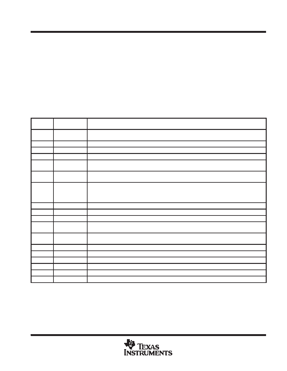
Table 5. Explanation of Timing Example
TCK
CYCLE(S)
TAP STATE
AFTER TCK
DESCRIPTION
1
Test-Logic-Reset
TMS is changed to a logic 0 value on the falling edge of TCK to begin advancing the TAP controller toward
the desired state.
2
Run-Test/Idle
3
Select-DR-Scan
4
Select-IR-Scan
5
Capture-IR
The IR captures the 8-bit binary value 10000001 on the rising edge of TCK as the TAP controller exits the
Capture-IR state.
6
Shift-IR
TDO becomes active and TDI is made valid on the falling edge of TCK. The first bit is shifted into the TAP
on the rising edge of TCK as the TAP controller advances to the next state.
7–13
Shift-IR
One bit is shifted into the IR on each TCK rising edge. With TDI held at a logic 1 value, the 8-bit binary value
11111111 is serially scanned into the IR. At the same time, the 8-bit binary value 10000001 is serially scanned
out of the IR via TDO. In TCK cycle 13, TMS is changed to a logic 1 value to end the IR scan on the next
TCK cycle. The last bit of the instruction is shifted as the TAP controller advances from Shift-IR to Exit1-IR.
14
Exit1-IR
TDO becomes inactive (goes to the high-impedance state) on the falling edge of TCK.
15
Update-IR
The IR is updated with the new instruction (BYPASS) on the falling edge of TCK.
16
Select-DR-Scan
17
Capture-DR
The bypass register captures a logic 0 value on the rising edge of TCK as the TAP controller exits the
Capture-DR state.
18
Shift-DR
TDO becomes active and TDI is made valid on the falling edge of TCK. The first bit is shifted into the TAP
on the rising edge of TCK as the TAP controller advances to the next state.
19–20
Shift-DR
The binary value 101 is shifted in via TDI, while the binary value 010 is shifted out via TDO.
21
Exit1-DR
TDO becomes inactive (goes to the high-impedance state) on the falling edge of TCK.
22
Update-DR
The selected data register is updated with the new data on the falling edge of TCK.
23
Select-DR-Scan
24
Select-IR-Scan
25
Test-Logic-Reset
Test operation completed
相關(guān)PDF資料 |
PDF描述 |
|---|---|
| 74LVX573MTR | LV/LV-A/LVX/H SERIES, 8-BIT DRIVER, TRUE OUTPUT, PDSO20 |
| 74VHC03TTR | AHC/VHC SERIES, QUAD 2-INPUT NAND GATE, PDSO14 |
| 74VHC112M | Dual J-K Flip-Flops with Preset and Clear |
| 74VHC112MTC | Dual J-K Flip-Flops with Preset and Clear |
| 74VHC112SJ | Dual J-K Flip-Flops with Preset and Clear |
相關(guān)代理商/技術(shù)參數(shù) |
參數(shù)描述 |
|---|---|
| 74LVTH182646APMG4 | 功能描述:特定功能邏輯 3.3V ABT Scan Test Devices RoHS:否 制造商:Texas Instruments 產(chǎn)品: 系列:SN74ABTH18502A 工作電源電壓:5 V 封裝 / 箱體:LQFP-64 封裝:Tube |
| 74LVTH182652APMG4 | 功能描述:特定功能邏輯 3.3V ABT Scan Test Devices RoHS:否 制造商:Texas Instruments 產(chǎn)品: 系列:SN74ABTH18502A 工作電源電壓:5 V 封裝 / 箱體:LQFP-64 封裝:Tube |
| 74LVTH18502APMRG4 | 功能描述:特定功能邏輯 3.3V ABT Scan Test Devices RoHS:否 制造商:Texas Instruments 產(chǎn)品: 系列:SN74ABTH18502A 工作電源電壓:5 V 封裝 / 箱體:LQFP-64 封裝:Tube |
| 74LVTH18504APMRG4 | 功能描述:特定功能邏輯 3.3V ABT Scan Test Devices RoHS:否 制造商:Texas Instruments 產(chǎn)品: 系列:SN74ABTH18502A 工作電源電壓:5 V 封裝 / 箱體:LQFP-64 封裝:Tube |
| 74LVTH18511DGGRE4 | 功能描述:總線收發(fā)器 3.3V ABT 18-BIT Univ Bus Transceiver RoHS:否 制造商:Fairchild Semiconductor 邏輯類型:CMOS 邏輯系列:74VCX 每芯片的通道數(shù)量:16 輸入電平:CMOS 輸出電平:CMOS 輸出類型:3-State 高電平輸出電流:- 24 mA 低電平輸出電流:24 mA 傳播延遲時(shí)間:6.2 ns 電源電壓-最大:2.7 V, 3.6 V 電源電壓-最小:1.65 V, 2.3 V 最大工作溫度:+ 85 C 封裝 / 箱體:TSSOP-48 封裝:Reel |
發(fā)布緊急采購,3分鐘左右您將得到回復(fù)。