- 您現(xiàn)在的位置:買賣IC網(wǎng) > PDF目錄360489 > 74LV4316N (NXP SEMICONDUCTORS) STANDARD GAIN HORN; WAVEGUIDE SIZE: WR28; FREQUENCY RANGE: 26.50-40.00; GAIN: 15 dB PDF資料下載
參數(shù)資料
| 型號: | 74LV4316N |
| 廠商: | NXP SEMICONDUCTORS |
| 元件分類: | 多路復(fù)用及模擬開關(guān) |
| 英文描述: | STANDARD GAIN HORN; WAVEGUIDE SIZE: WR28; FREQUENCY RANGE: 26.50-40.00; GAIN: 15 dB |
| 中文描述: | QUAD 1-CHANNEL, SGL POLE SGL THROW SWITCH, PDIP16 |
| 文件頁數(shù): | 8/16頁 |
| 文件大小: | 156K |
| 代理商: | 74LV4316N |
Philips Semiconductors
Product specification
74LV4316
Quad bilateral switches
1998 Jun 23
8
ADDITIONAL AC CHARACTERISTICS
GND = 0 V; t
r
= t
f
≤
2.5ns; C
L
= 50pF
SYMBOL
PARAMETER
TYP
UNIT
V
CC
(V)
3.0
6.0
3.0
6.0
3.0
6.0
3.0
6.0
V
IS(P–P)
(V)
2.75
5.50
2.75
5.50
Note 1
CONDITIONS
Sine-wave distortion f = 1 kHz
0.80
0.40
2.40
1.20
–50
–50
–60
–60
%
R
= 10 k ; C
= 50 pF
L
Figure 10
L
Sine-wave distortion f = 10 kHz
%
R
= 10 k ; C
= 50 pF
Figure 10
L
Switch “OFF” signal feed through
Switch OFF signal feed through
dB
R
= 600 k ; C
= 50 pF; f=1 MHz
L
L
Figures 5 and 11
Crosstalk between any two switches
dB
Note 1
R
= 600 k ; C
= 50 pF; f=1 MHz
L
Figure 7
R
L
= 600 k ; C
L
= 50 pF; f=1 MHz
(nS or E square wave between V
(nS or E, square wave between V
CC
and GND, T
r
= t
f
= 6 ns) Figure 8
R
= 50 k ; C
= 50 pF
L
L
Figures 6 and 9
V
(p–p)
Crosstalk voltage between enable or address
input to any switch (peak-to-peak value)
110
mV
3.0
220
6.0
f
max
Minimum frequency response (–3 dB)
Minimum frequency res onse (–3 dB)
180
200
5
mHz
3.0
6.0
Note 2
C
S
Maximum switch capacitance
GENERAL NOTES:
V
is
is the input voltage at nY or nZ terminal, whichever is assigned as an input.
V
os
is the output voltage at nY or nZ terminal, whichever is assigned as an output.
NOTES:
1. Adjust input voltage V
is
is 0 dBm level (0 dBm = 1 mW into 600 ).
2. Adjust input voltage V
is
is 0 dBm level at V
os
for 1 MHz (0 dBm = 1 mW into 50 ).
pF
SV01635
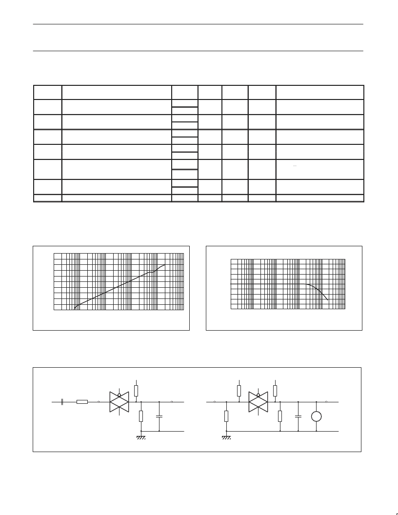
(dB)
f (kHz)
0
10
10
2
10
3
10
4
10
5
10
6
–50
–100
Figure 5. Typical switch “OFF” signal feed-through as a
function of frequency.
SV01664
(dB)
f (kHz)
5
10
102
103
104
105
106
0
–
5
Figure 6. Typical frequency response.
NOTES TO FIGURES 5 AND 6:
Test conditions: V
CC
= 3.0 V; GND = 0 V; R
L
= 50 ; R
SOURCE
= 1k .
SV01665
GND
2R
L
V
CC
channel
ON
Vis
0.1 F
R
L
nY/nZ
nZ/nY
C
L
GND
channel
OFF
(b)
(a)
V
os
dB
2R
L
nY/nZ
2R
L
2R
L
V
CC
V
CC
nZ/nY
2R
L
C
L
R
L
Figure 7. Test circuit for measuring crosstalk between any two switches.
(a) channel ON condition; (b) channel OFF condition.
相關(guān)PDF資料 |
PDF描述 |
|---|---|
| 74LV4316PW | STANDARD GAIN HORN; WAVEGUIDE SIZE: WR28; FREQUENCY RANGE: 26.50-40.00; GAIN: 20 dB |
| 74LV4316PWDH | STANDARD GAIN HORN; WAVEGUIDE SIZE: WR34; FREQUENCY RANGE: 22.00-33.00; GAIN: 10 dB |
| 74LV4799PW | Timer for NiCd and NiMH chargers |
| 74LV4799PWDH | Timer for NiCd and NiMH chargers |
| 74LV4799 | Timer for NiCd and NiMH chargers(為 NiCd和NiMH 充電的定時器) |
相關(guān)代理商/技術(shù)參數(shù) |
參數(shù)描述 |
|---|---|
| 74LV4316PW | 制造商:PHILIPS 制造商全稱:NXP Semiconductors 功能描述:Quad bilateral switches |
| 74LV4316PWDH | 制造商:PHILIPS 制造商全稱:NXP Semiconductors 功能描述:Quad bilateral switches |
| 74LV4316PW-T | 制造商:未知廠家 制造商全稱:未知廠家 功能描述:SPST Analog Switch |
| 74LV4799 | 制造商:PHILIPS 制造商全稱:NXP Semiconductors 功能描述:Timer for NiCd and NiMH chargers |
| 74LV4799D | 功能描述:計時器和支持產(chǎn)品 3.3V TIMER NICD AND NIMH CHARGER RoHS:否 制造商:Micrel 類型:Standard 封裝 / 箱體:SOT-23 內(nèi)部定時器數(shù)量:1 電源電壓-最大:18 V 電源電壓-最小:2.7 V 最大功率耗散: 最大工作溫度:+ 85 C 最小工作溫度:- 40 C 封裝:Reel |
發(fā)布緊急采購,3分鐘左右您將得到回復(fù)。